Visual inspection and verification system

a verification system and visual inspection technology, applied in the field of integrated circuit manufacturing, can solve the problems of not being able to perfectly reproduce the design serif 215 shape on the mask material, affecting the quality of mask materials, and being unrealistic to assum

Inactive Publication Date: 2004-12-02
SYNOPSYS INC
View PDF9 Cites 80 Cited by
  • Summary
  • Abstract
  • Description
  • Claims
  • Application Information

AI Technical Summary

Problems solved by technology

It is, unfortunately, unrealistic to assume that the electron beam and other machines used to manufacture these masks can do so without error.
In the typical manufacturing process, some mask defects do occur outside the controlled process.
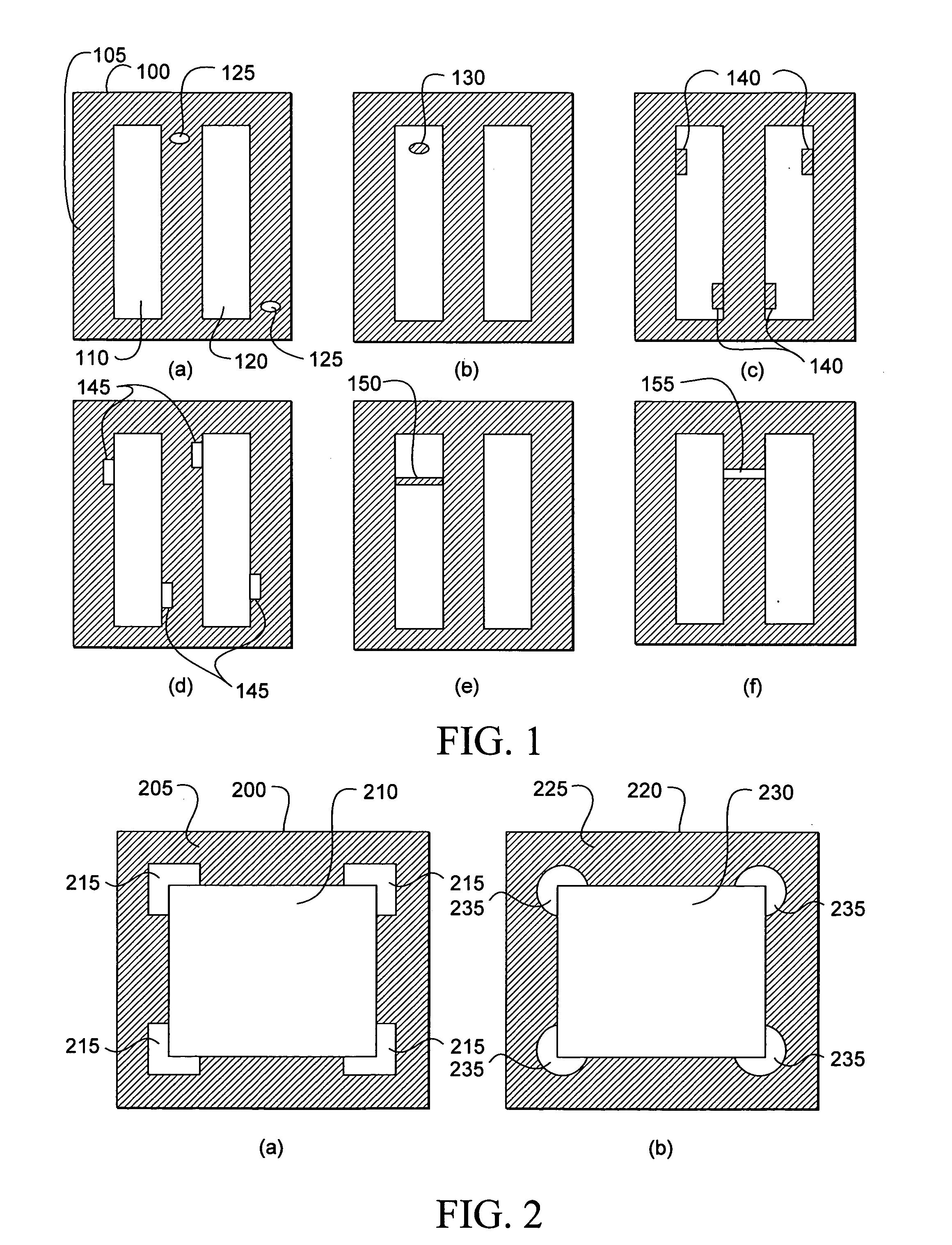
This is because the size of the serifs is very small--they are designed to be smaller than the optical resolution of the lithography process to be used--and the electron beam typically can not perfectly reproduce the design serif 215 shape onto the mask material.
However, not all mask defects are important with respect to the desired end result--the end result being an accurate representation of the original design layout on the photoresist material or etched into silicon.
Due to these changes, conventional methods of inspection are rapidly proving to be inadequate because they do not address several issues.
First, whether a defect prints or not greatly depends on both its location and size, not just size or transmission / reflection characteristics alone.
Second, advanced OPC mask features can trigger false defect detections.
Although some existing mask inspection tools have a sliding scale setting to "tolerate" OPC features, this is not a robust method since defects associated with these special features may be overlooked because of this arbitrary scale.
Additionally, OPC features are typically designed for a specific set of stepper parameters, but conventional tools' sliding scales are blind to these optical parameters.
Third, phase information is not properly incorporated into consideration, if at all, in the typical conventional defect inspection scheme.
Therefore, phase shifting masks are not properly inspected.
Finally, even though a defect may not appear to print, it might affect the process latitude in a way that will decrease yield and not be detected by conventional on-line defect inspection systems.
On the other hand, off-line inspection stations, which either scan for defects directly or review previously stored undeterminable defect data from an on-line tool, also face the same issues.
In addition, these issues may require expensive engineers' time to be resolved, and thus diminish throughput while raising cost.
Although with an engineer's judgement, magnitude of the defect printability / classification problem is greatly reduced due to experience and know-how, still, there is not enough certainty and accuracy until the defect is viewed as it appears on an actual wafer after exposure through the mask.
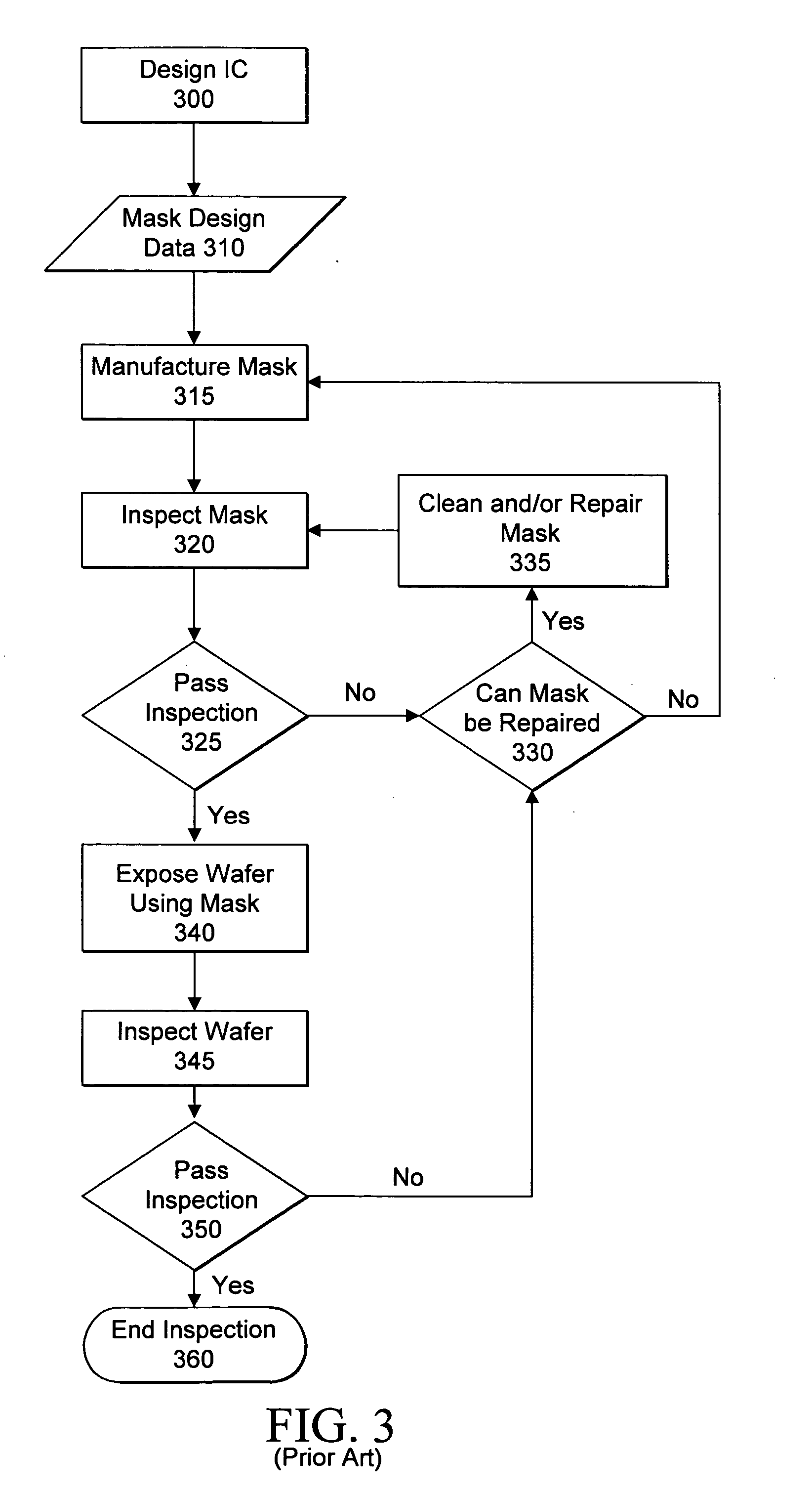
Thus, using currently existing inspection systems, it is nearly impossible to judge a defect's printability without actually printing the mask onto a wafer, which is expensive and time-consuming.
As discussed above, currently known mask inspection systems are not capable of providing an accurate measure of the printability of a potential mask defect and / or overall mask quality assessment without resorting to an actual exposure of a wafer with the mask in question.

Method used


Image

  • Visual inspection and verification system
  • Visual inspection and verification system
  • Visual inspection and verification system

Examples


Embodiment Construction

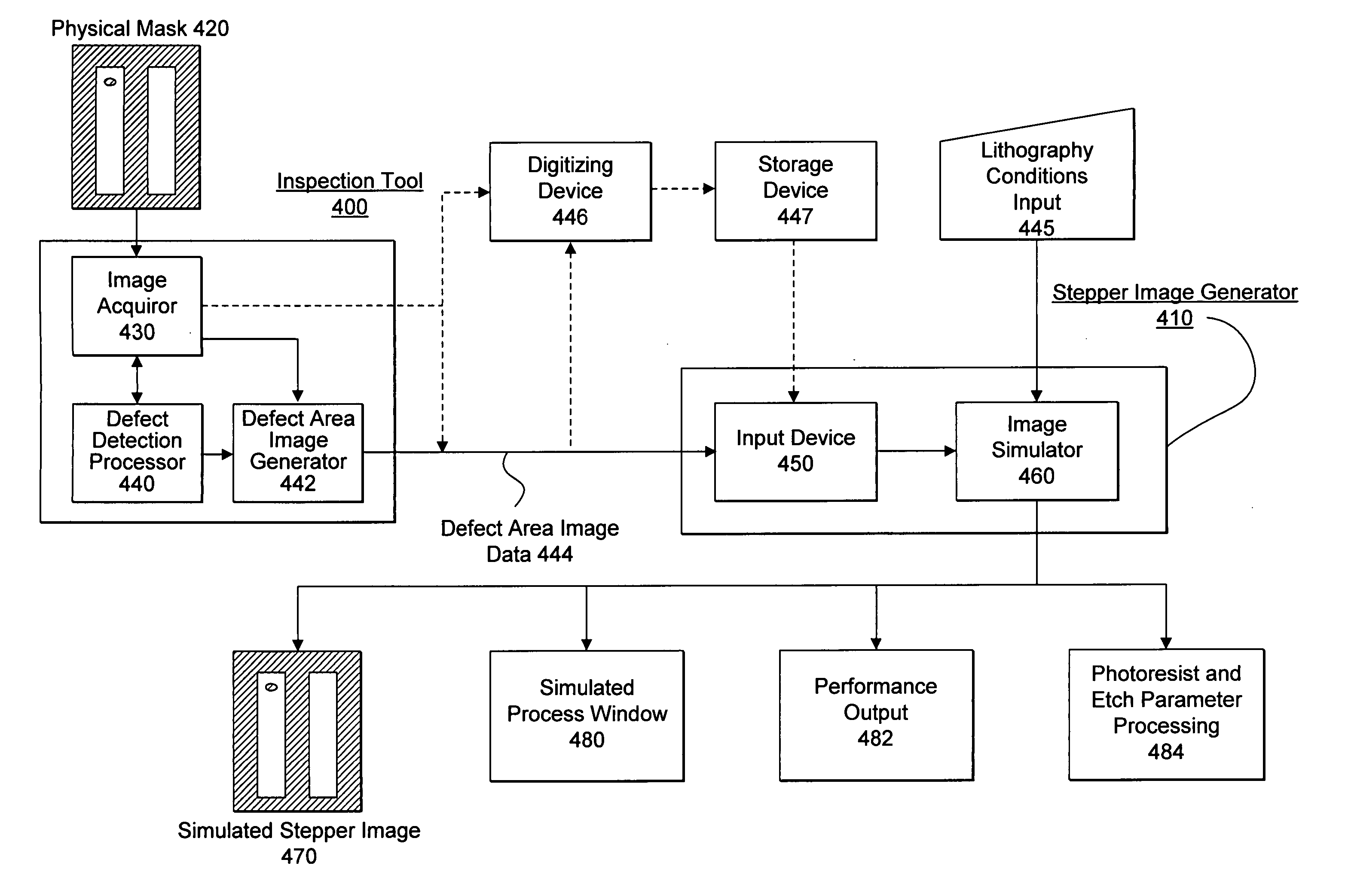
[0067] Photolithography is a process whose input is a mask and whose output is the printed patterns on a wafer. The printed result from a mask is what design engineers, lithographers, and mask manufacturers really care about. Using prior methods, the only way to inspect this printed result was to perform an actual wafer exposure and therefore incur potentially unnecessary costs in time and money. The present invention solves some of the problems of these prior methods by providing for mask inspection that takes printability into account without the need for the expensive steps of actually exposing a wafer. The present invention is capable of using a captured image of a mask--that accurately enough represents the physical mask (i.e. such as from a high resolution optical microscope or a scanning electron microscope)--and using that captured image to simulate the wafer exposure that the mask would provide under a given set of stepper conditions. Thus, when an initial mask inspection f...


PUM

PropertyMeasurementUnit
areaaaaaaaaaaa
defect areaaaaaaaaaaa
potential defectaaaaaaaaaa

Abstract

A method and apparatus for inspecting a photolithography mask for defects is provided. The inspection method comprises providing a defect area image to an image simulator wherein the defect area image is an image of a portion of a photolithography mask, and providing a set of lithography parameters as a second input to the image simulator. The defect area image may be provided by an inspection tool which scans the photolithography mask for defects using a high resolution microscope and captures images of areas of the mask around identified potential defects. The image simulator generates a first simulated image in response to the defect area image and the set of lithography parameters. The first simulated image is a simulation of an image which would be printed on a wafer if the wafer were to be exposed to an illumination source directed through the portion of the mask. The method may also include providing a second simulated image which is a simulation of the wafer print of the portion of the design mask which corresponds to the portion represented by the defect area image. The method also provides for the comparison of the first and second simulated images in order to determine the printability of any identified potential defects on the photolithography mask. A method of determining the process window effect of any identified potential defects is also provided for.

Description

[0001] This application is a continuation of U.S. patent application Ser. No. 09 / 130,996 filed 7 Aug. 1998, which will issue as U.S. Pat. No. 6,757,645 on 29 Jun. 2004.[0002] This application relates to, claims benefit of the filing date of, and incorporates by reference, the U.S. provisional patent application entitled, "Mask Verification, Correction, and Design Rule Checking" having Ser. No. 60 / 059,306, filed Sep. 17, 1997, invented by Fang-Cheng Chang, Yao-Ting Wang and Yagyensh C. Pati, and assigned to the assignee of the present invention.THE BACKGROUND OF THE INVENTION[0003] 1. The Field of the Invention[0004] This invention relates to the field of integrated circuit manufacturing. In particular, the invention relates to a system for inspection of defects on masks used in the manufacture of integrated circuits.[0005] 2. Description of Related Art[0006] In designing an integrated circuit (IC), engineers typically rely upon computer simulation tools to help create a circuit sche...

Claims


Application Information

Patent Timeline
Patent Type & Authority Applications(United States)
IPC IPC(8): G01Q30/02G01Q30/04G01Q60/18G01Q60/24G01Q80/00G01Q90/00G03F1/26G03F1/36G03F1/84G03F7/14G03F7/20G06F17/50G06T7/00H01L21/027
CPCG03F1/26G03F1/36G03F1/84G03F7/70441G03F7/705G06F17/5068G06T7/0004G06T2207/30148G06F30/39G06F18/00
Inventor CHANG, FANG-CHENGWANG, YAO-TINGPATI, YAGYENSH C.KARKLIN, LINARD N.
Owner SYNOPSYS INC
Why Eureka
Try Eureka