Design flow for shrinking circuits having non-shrinkable IP layout

a design flow and layout technology, applied in the field of shrinking integrated circuits, can solve the problems of not being able to uniformly shrink the integrated circuit of a semiconductor chip, not being able to cost effective redesign these circuits for smaller dimensions, and circuits that were typically shrunk, etc., to achieve the effect of changing the size and location of components

Inactive Publication Date: 2008-09-18
TAIWAN SEMICON MFG CO LTD
View PDF2 Cites 7 Cited by
  • Summary
  • Abstract
  • Description
  • Claims
  • Application Information

AI Technical Summary

Benefits of technology

[0011]In the embodiments of the present invention, the IP layouts of the non-shrinkable integrated circuits are not shrunk. The adverse effects caused by the shrinking of the non-shrinkable integrated circuits, such as the change in sizes and locations of components, are thus reduced, and possibly eliminated.

Problems solved by technology

It is not cost effective to redesign these circuits for smaller dimensions, and these circuits were typically shrunk before they are implemented on silicon wafers.
This creates a dilemma.
Since these non-shrinkable integrated circuits are often integrated in the same semiconductor chips with shrinkable integrated circuits, whose performances are not affected by their dimensions, the integrated circuits for a semiconductor chip cannot be uniformly shrunk, and efforts are needed to shrink only the shrinkable circuits, while keeping the non-shrinkable circuits intact.
The conventional methods for shrinking integrated circuits suffer drawbacks, however.
First, even if the non-shrinkable circuits are magnified and then shrunk in a same scale, the resulting dimensions and locations of the final circuits may not be exactly the same as in the original design.
This is due to the snapping of integrated circuits to grids, which causes the change in the size and / or location of integrated circuit components.
The change in dimensions may cause performance drift.
Second, GDS files are typically hierarchical with a plurality of levels.
This causes the handling time to be longer.
Third, the adverse change in the dimensions of integrated circuits due to the snapping causes device mismatching.

Method used


Image

  • Design flow for shrinking circuits having non-shrinkable IP layout
  • Design flow for shrinking circuits having non-shrinkable IP layout
  • Design flow for shrinking circuits having non-shrinkable IP layout

Examples


Embodiment Construction

[0017]The making and using of the presently preferred embodiments are discussed in detail below. It should be appreciated, however, that the present invention provides many applicable inventive concepts that can be embodied in a wide variety of specific contexts. The specific embodiments discussed are merely illustrative of specific ways to make and use the invention, and do not limit the scope of the invention.

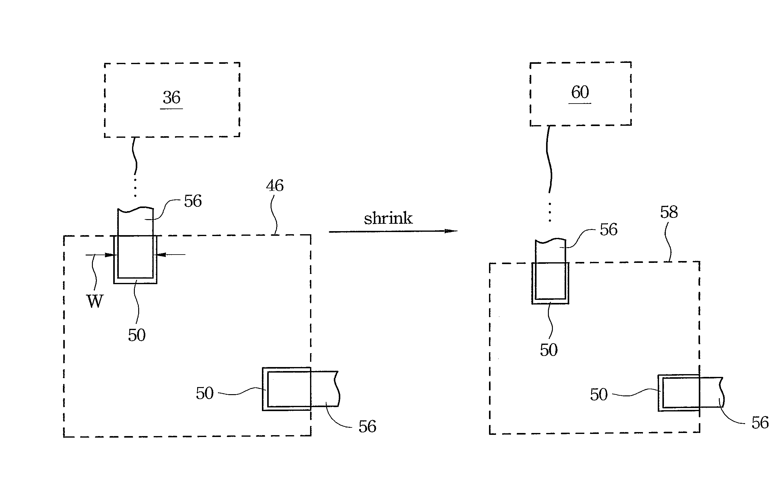
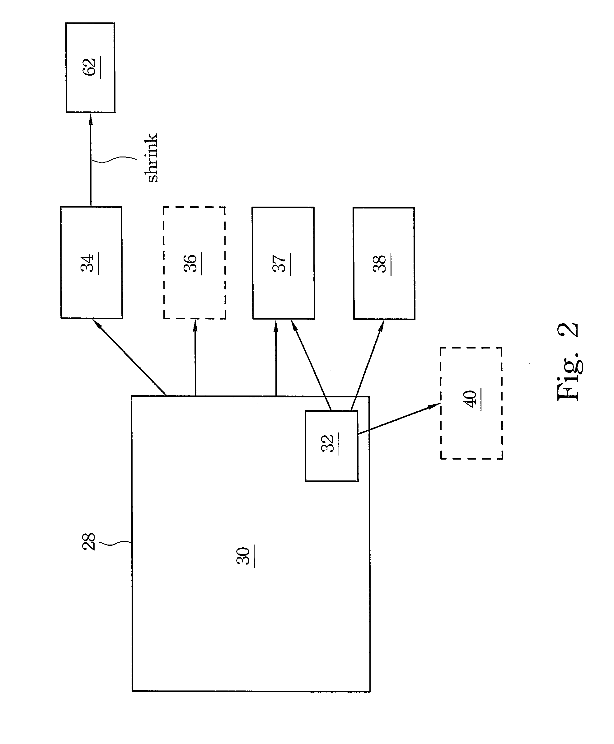
[0018]FIGS. 1 through 4 illustrate an embodiment of the present invention, in which integrated circuits designed using 45 nm scale is shrunk to 40 nm scale. It is noted that the 45 nm scale and 40 nm scale are merely examples, and the teaching of the present invention may be used for the shrinking of integrated circuits between any two technology generations.

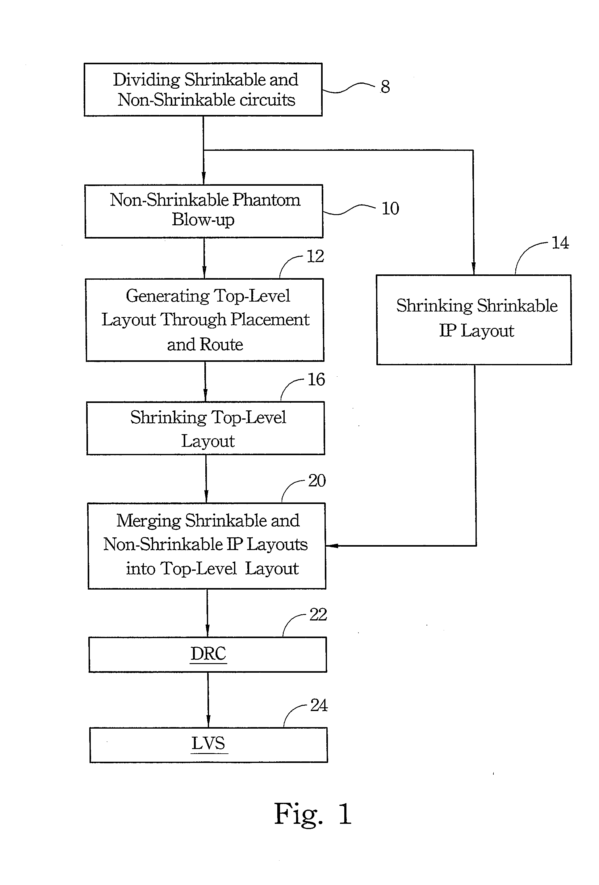
[0019]FIG. 1 illustrates an exemplary flow chart. The steps recited in the flow chart are discussed in detail in the subsequent paragraphs. For simplicity, the embodiments of the present invention recites the scale of 10 / ...


PUM


Abstract

A method for processing an integrated circuit is provided. The method includes providing a first integrated circuit having a first scale, wherein the first integrated circuit comprises a shrinkable circuit comprising a first intellectual property (IP) layout, and a non-shrinkable circuit comprising a second IP layout; and generating a second integrated circuit having a second scale smaller than the first scale. The step of generating the second integrated circuit includes shrinking the shrinkable integrated circuit to the second scale. The method further includes merging the second IP layout with the non-shrinkable circuit to generate a final integrated circuit.

Description

[0001]This application claims the benefit of U.S. Provisional Application Ser. No. 60 / 906,794, filed on Mar. 13, 2007, entitled “Shrink Design Flow with Don't Touch Critical (or Legacy) IP Layout,” which application is hereby incorporated herein by reference.TECHNICAL FIELD[0002]This invention relates generally to the manufacture of integrated circuits, and more particularly to the shrinking of integrated circuits between different technology generations.BACKGROUND[0003]In order to incorporate more functions and achieve better performance and less cost, integrated circuits are formed with increasingly smaller dimensions. However, there are legacy circuits that have already been designed with greater dimensions. It is not cost effective to redesign these circuits for smaller dimensions, and these circuits were typically shrunk before they are implemented on silicon wafers. Conventionally, foundries performed the task of shrinking integrated circuits.[0004]Since the performances of in...

Claims


Application Information

Patent Timeline
Patent Type & Authority Applications(United States)
IPC IPC(8): G06F17/50
CPCG06F17/5068G06F17/5045G06F30/30G06F30/39G06F2115/08
Inventor WANG, CHUNG-HSINGLU, LEE-CHUNGHOU, CLIFFJUANG, LIE-SZU
Owner TAIWAN SEMICON MFG CO LTD
Why Eureka
Try Eureka