

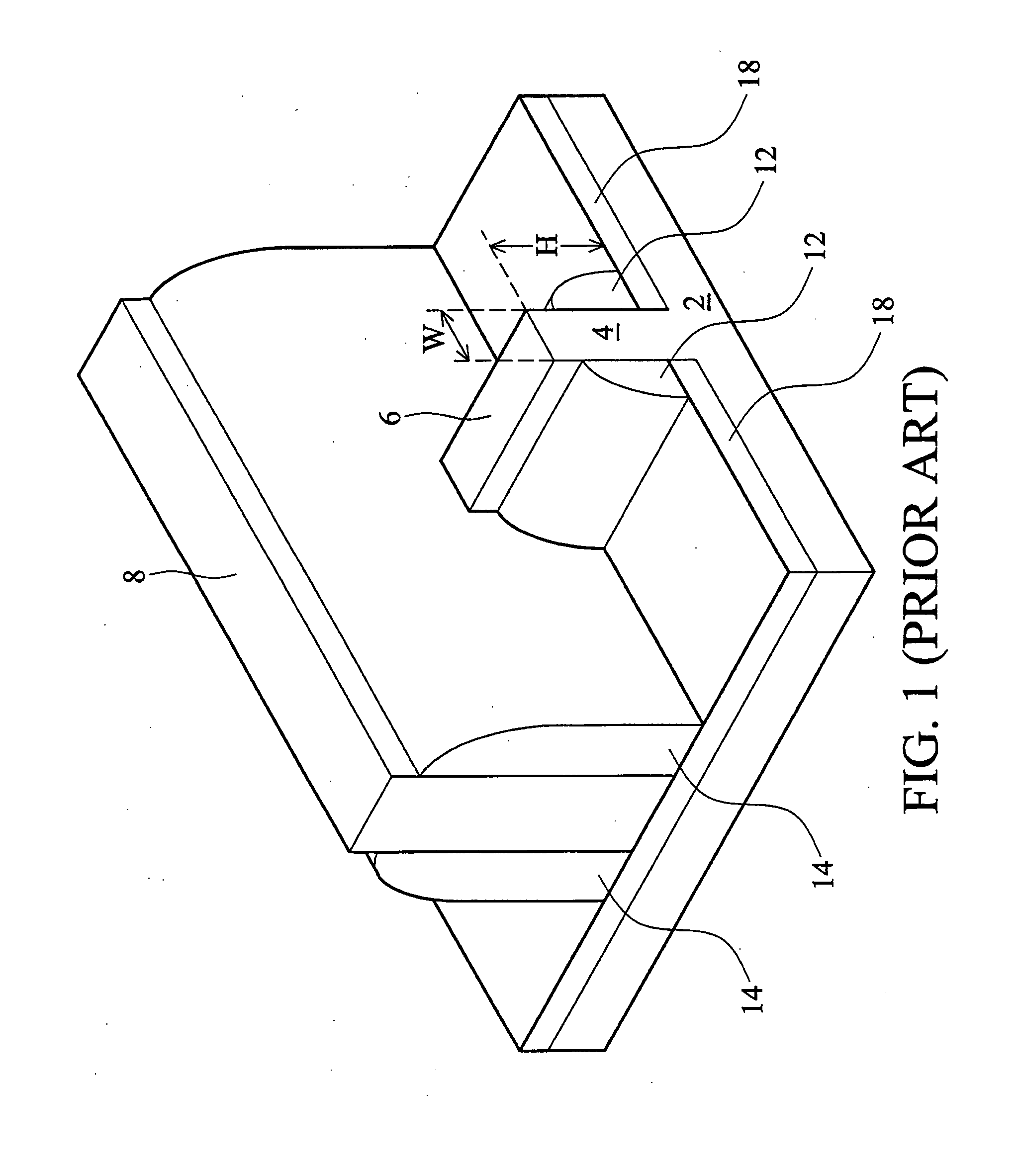
Fabrication of FinFETs with multiple fin heights
a technology of fin height and fin height, which is applied in the direction of semiconductor devices, electrical equipment, transistors, etc., can solve the problems of limiting the capability for customizing the performance of finfets, increasing gate widths, and conflicting with the requirements of reducing the size of semiconductor devices
- Summary
- Abstract
- Description
- Claims
- Application Information
AI Technical Summary
Benefits of technology
Problems solved by technology
Method used
Image

Examples
Embodiment Construction
[0018]The making and using of the presently preferred embodiments are discussed in detail below. It should be appreciated, however, that the present invention provides many applicable inventive concepts that can be embodied in a wide variety of specific contexts. The specific embodiments discussed are merely illustrative of specific ways to make and use the invention, and do not limit the scope of the invention.
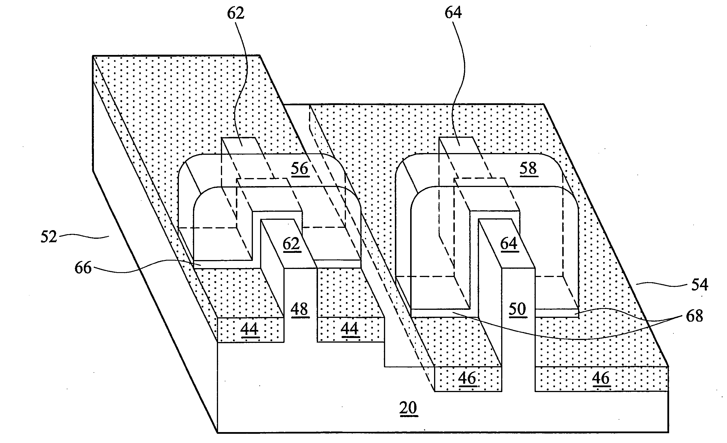
[0019]A novel method for forming semiconductor fins with different heights on a same semiconductor chip is provided. The intermediate stages of manufacturing a preferred embodiment of the present invention are illustrated. Throughout the various views and illustrative embodiments of the present invention, like reference numbers are used to designate like elements.
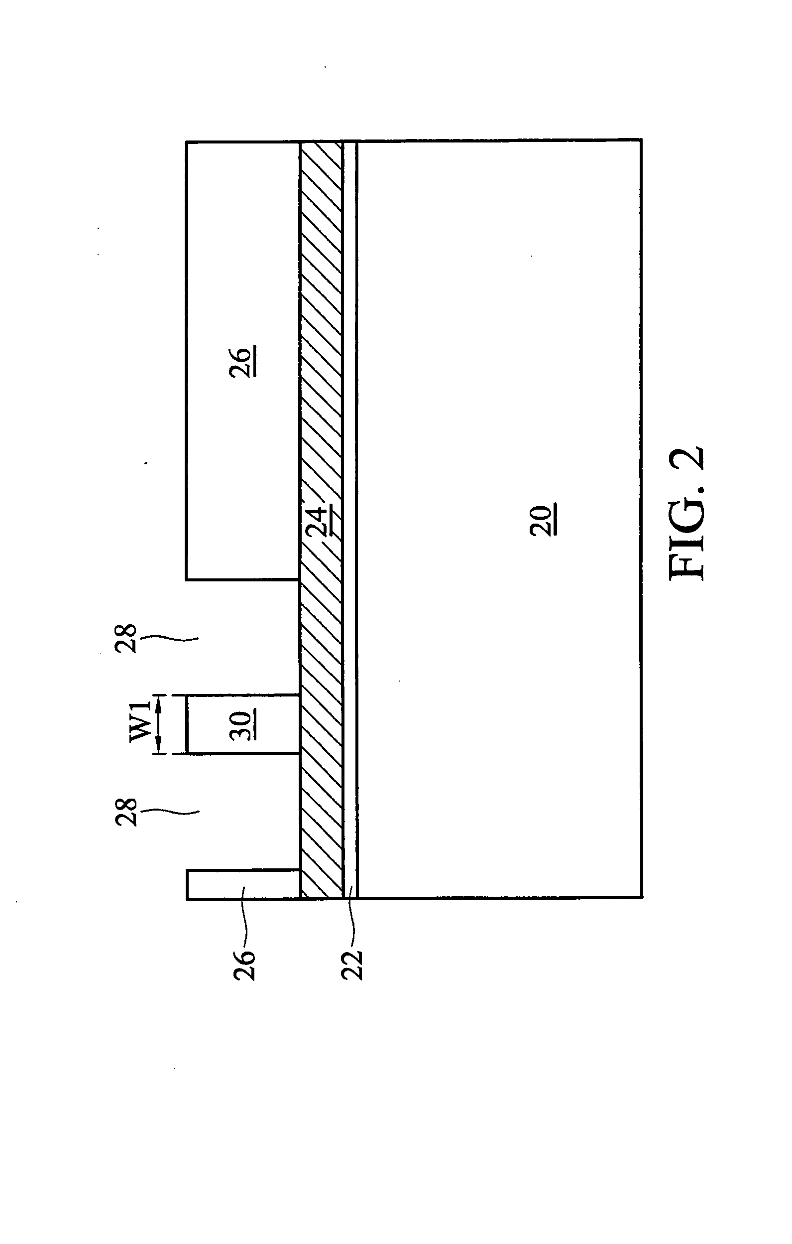
[0020]Referring to FIG. 2, semiconductor substrate 20 is provided. In the preferred embodiment, semiconductor substrate 20 includes silicon. Other commonly used materials, such as carbon, germanium, gallium, arsenic,...
PUM
 Abstract
Description
Claims
Application Information