

Nonvolatile semiconductor memory and method of manufacturing the same
Active Publication Date: 2008-10-02
KIOXIA CORP
View PDF2 Cites 15 Cited by
- Summary
- Abstract
- Description
- Claims
- Application Information
AI Technical Summary
Benefits of technology
[0012]An embodiment of the invention provides a nonvolatile semiconductor memory capable of enhancing the electric accumulating amount and increasing the threshold variation wid
Problems solved by technology
For the NAND flash memory, a flat-cell structure is needed because of difficulty in burying IPD (inter-poly dielectrics) in cells in the manufacturing process.
This is because, in the case of the FG structure for accumulating an electric charge in a metal gate film, if a local defect occurs in the tunnel film, the majority of the accumulated charge is lost through the defect.
In the technologies disclosed so far, at practical level, the charge accumulating amount of silicon nitride is not enough, and the threshold voltage change width is not sufficient.
If the silicon amount is increased in order to increase the charge accumulating amount, for example, the state become metallic, and the same problem as in the conventional FG structure occurs.
Further, when silicon nitride is used in the char
Method used
View moreImage
Smart ImageViewing Examples

Examples
 PUM
 Abstract
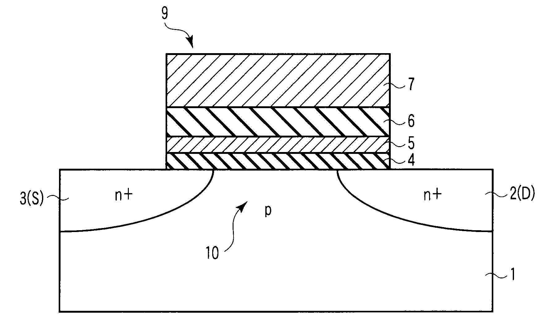
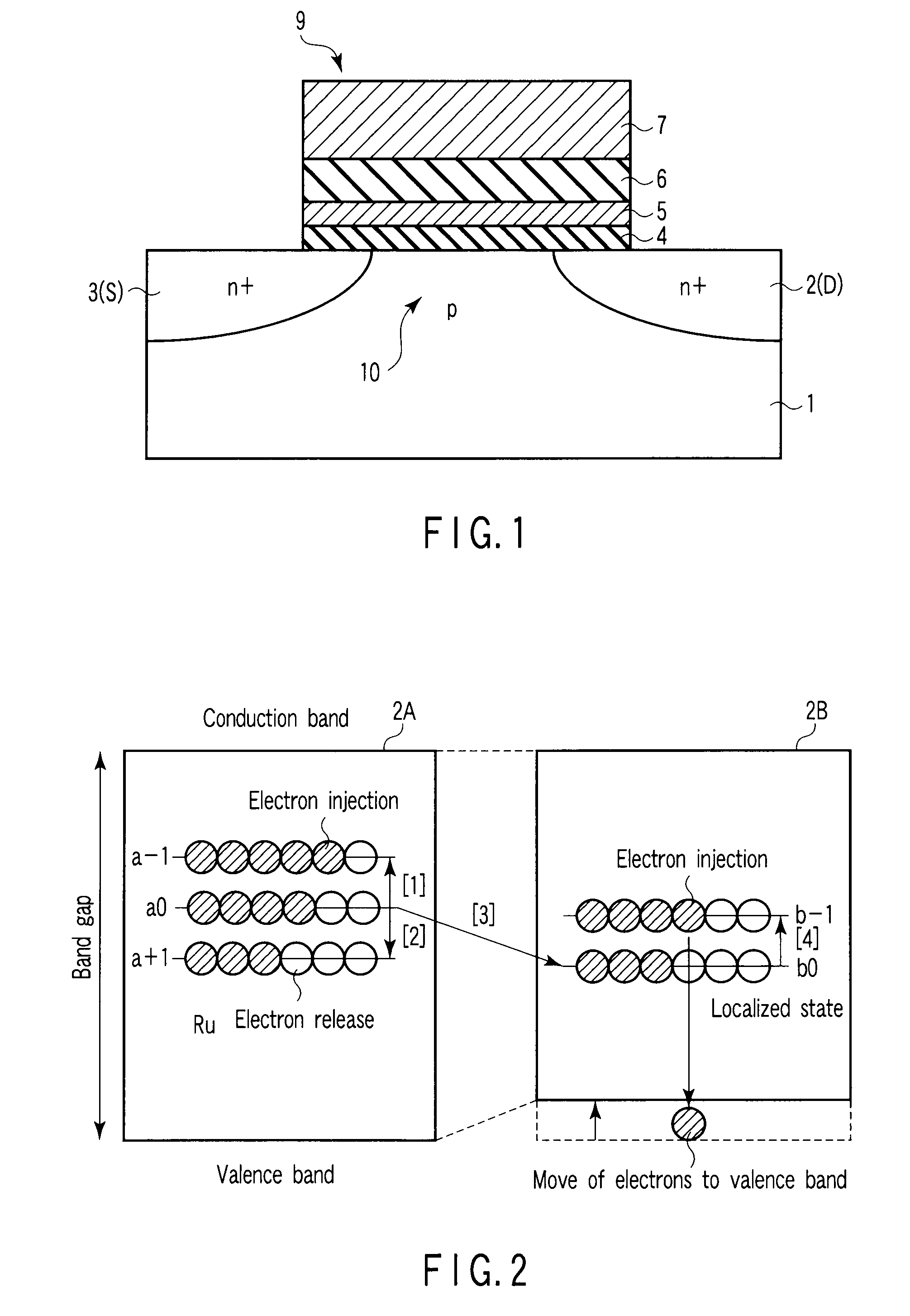
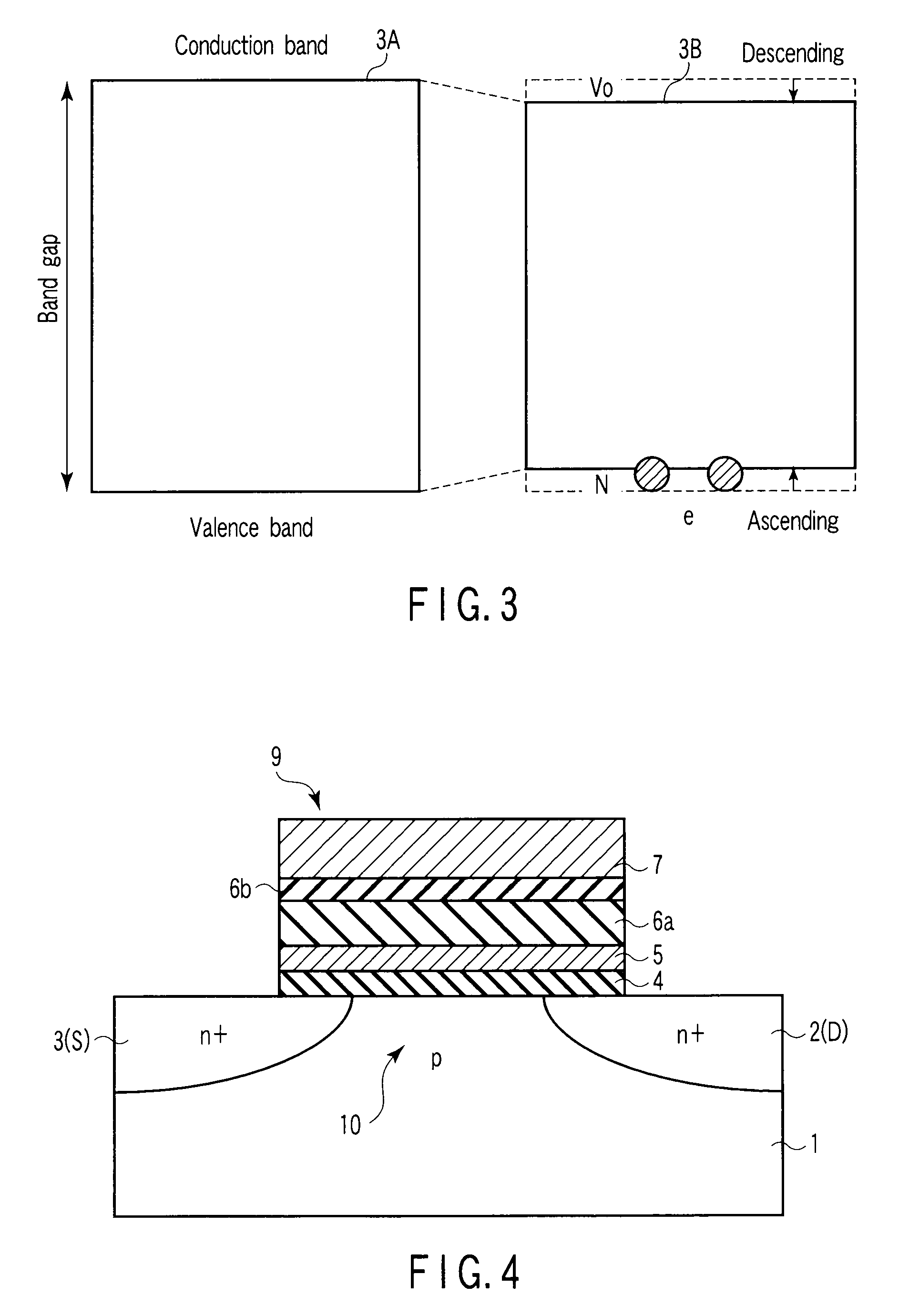
A metal oxide having a sufficiently higher dielectric constant than silicon nitride, such as Ti oxide, Zr oxide, or Hf oxide is used as base material, and in order to generate a trap level capable of moving in and out electrons therein, a high-valence substance of valence of 2 or more (that is, valence VI or higher) is added by a proper amount, and to control the trap level, a proper amount of nitrogen (carbon, boron, or low-valence substance) is added, and thus a nonvolatile semiconductor memory having a charge accumulating layer is obtained.
Description
CROSS-REFERENCE TO RELATED APPLICATIONS[0001]This application is based upon and claims the benefit of priority from prior Japanese Patent Application No. 2007-084275, filed Mar. 28, 2007, the entire contents of which are incorporated herein by reference.BACKGROUND OF THE INVENTION[0002]1. Field of the Invention[0003]The present invention relates to a nonvolatile semiconductor memory having an electric charge accumulating insulating film made of a high dielectric material, and a method of manufacturing the same.[0004]2. Description of the Related Art[0005]Generally, a flash memory is known as one of nonvolatile semiconductor memories, and it is widely used in electronic appliances. This flash memory does not require any electric holding action for storage (holding power supply), and programs can be easily written therein after the product is completed.[0006]A further finer structure and operation at a lower voltage are demanded in next-generation and future NAND flash memories. For t...
Claims
Login to View More Application Information
Patent Timeline
 IPC IPC(8): H01L29/792H01L21/336
CPCH01L21/28282H01L29/4234H01L29/513H01L29/66833H01L29/785H01L29/792H01L29/40117
InventorSHIMIZU, TATSUOMURAOKA, KOICHI
OwnerKIOXIA CORP