Flexible circuit electronic package with standoffs

a technology of electronic packages and standoffs, applied in the field of electronic packages, can solve the problems of increasing the cost of the final package, flex circuit warping, and being susceptible to bending

Inactive Publication Date: 2008-10-02
I3 ELECTRONICS
View PDF24 Cites 117 Cited by
  • Summary
  • Abstract
  • Description
  • Claims
  • Application Information

AI Technical Summary

Benefits of technology

[0025]According to another aspect of the invention, there is provided a method of making an electronic package comprising providing a heat sink, providing a flexible circuit including a plurality of conductors thereon, positioning a semiconductor chip on the flexible circuit and electrically coupling the chip to selected ones of the conductors, positioning a quantity of heat shrinkable adhesive in liquidus form between the flexible circuit and heat sink and in contact with both the flexible circuit and heat sink,...

Problems solved by technology

When positioning and electrically coupling a chip to a flex circuit using solder balls, some amount of flex circuit warping will occur, which is undesirable from both manufacturing and product functioning standpoints.
This warping occurs because the flex circuit is of an extremely thin (e.g., sometimes having an overall thickness of only about 8 mils (a ...

Method used


Image

  • Flexible circuit electronic package with standoffs
  • Flexible circuit electronic package with standoffs
  • Flexible circuit electronic package with standoffs

Examples


Embodiment Construction

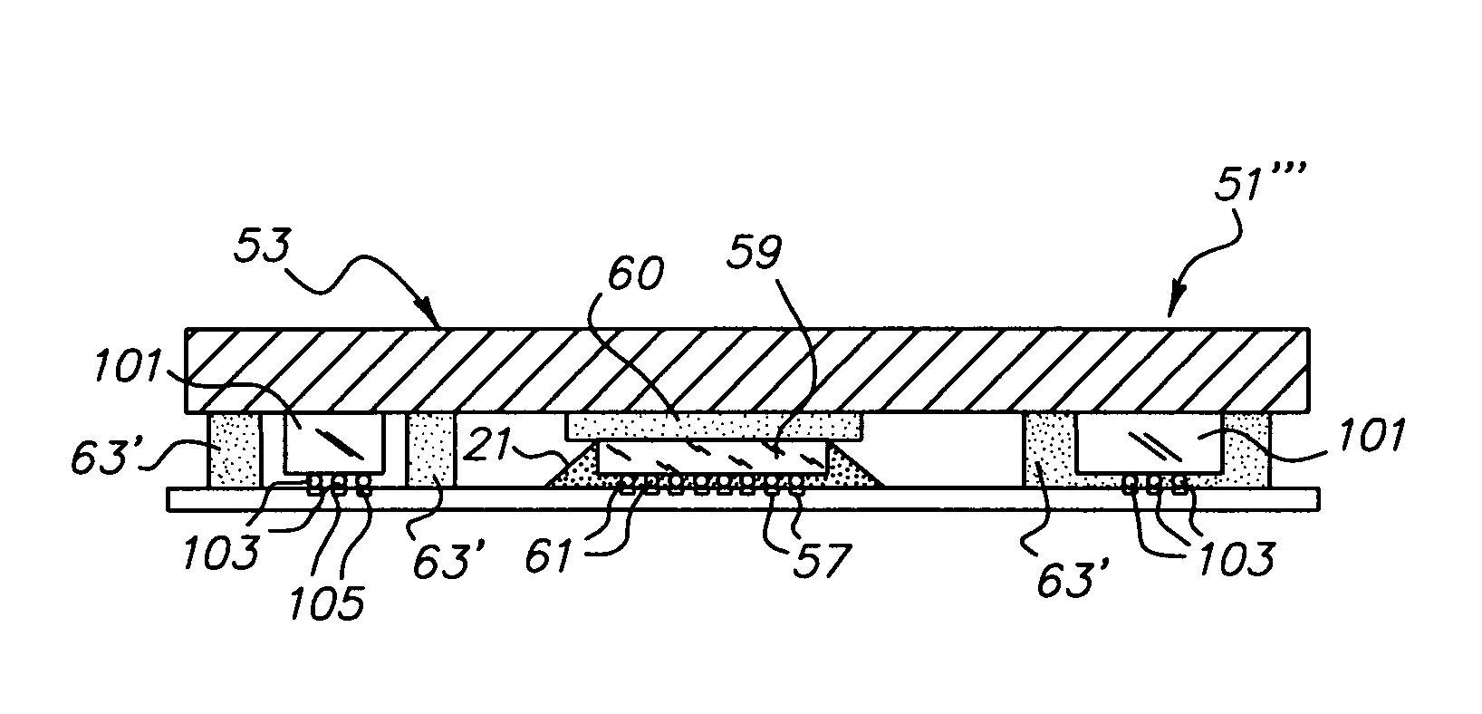
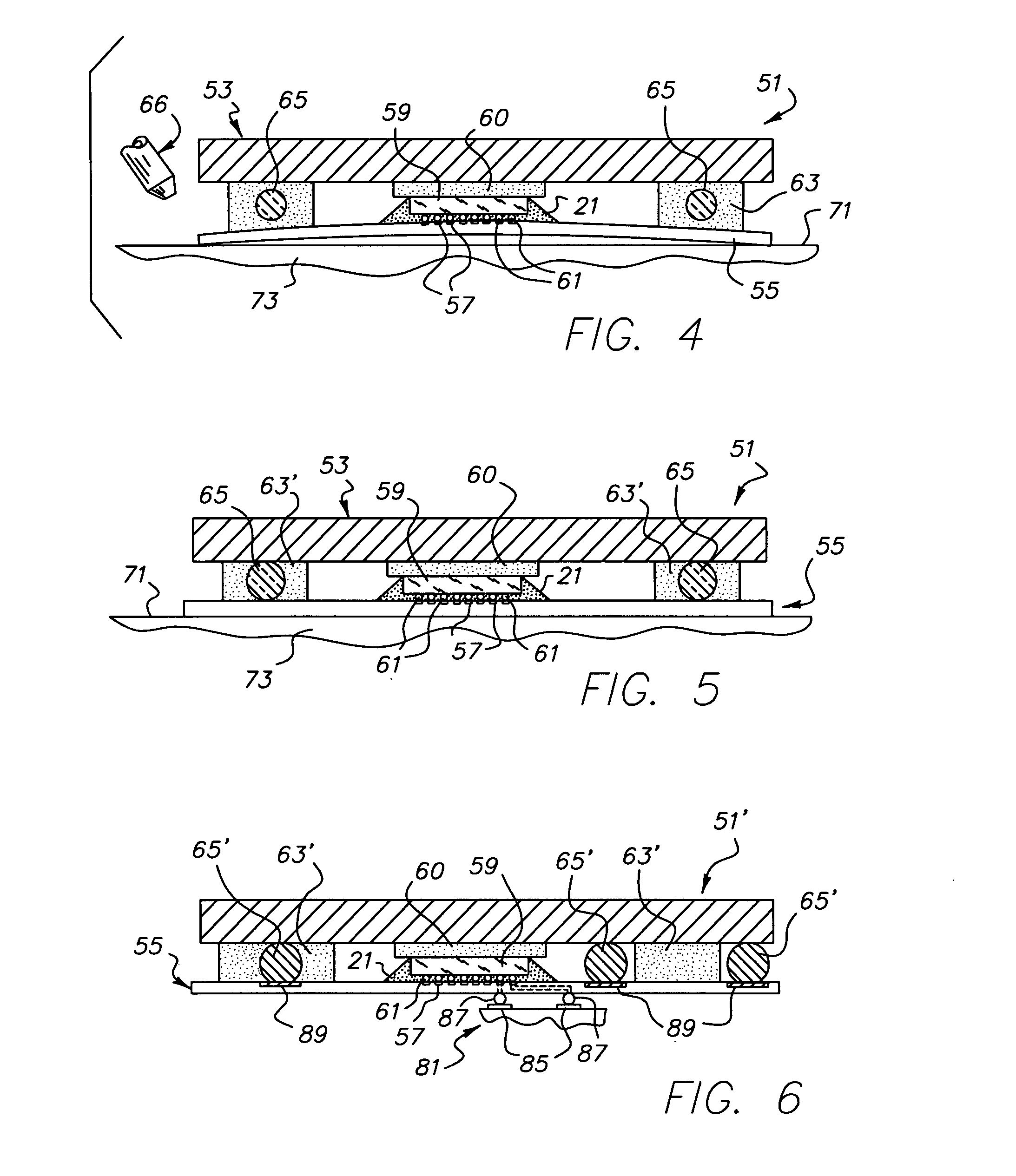
[0029]For a better understanding of the present invention, together with other and further objects, advantages and capabilities thereof, reference is made to the following disclosure and appended claims in connection with the above-described drawings. It is understood that like numerals will be used to indicate like elements from FIG. to FIG.

[0030]By the term “electrical assembly” as used herein is meant the combination of at least one electronic package and at least one printed circuit board (or PCB), the package positioned on and electrically coupled to the printed circuit board.

[0031]By the term “electronic package” as used herein is meant at least one flexible (or flex) circuit having at least one semiconductor chip thereon and at least one heat sink, the chip being thermally coupled to the heat sink.

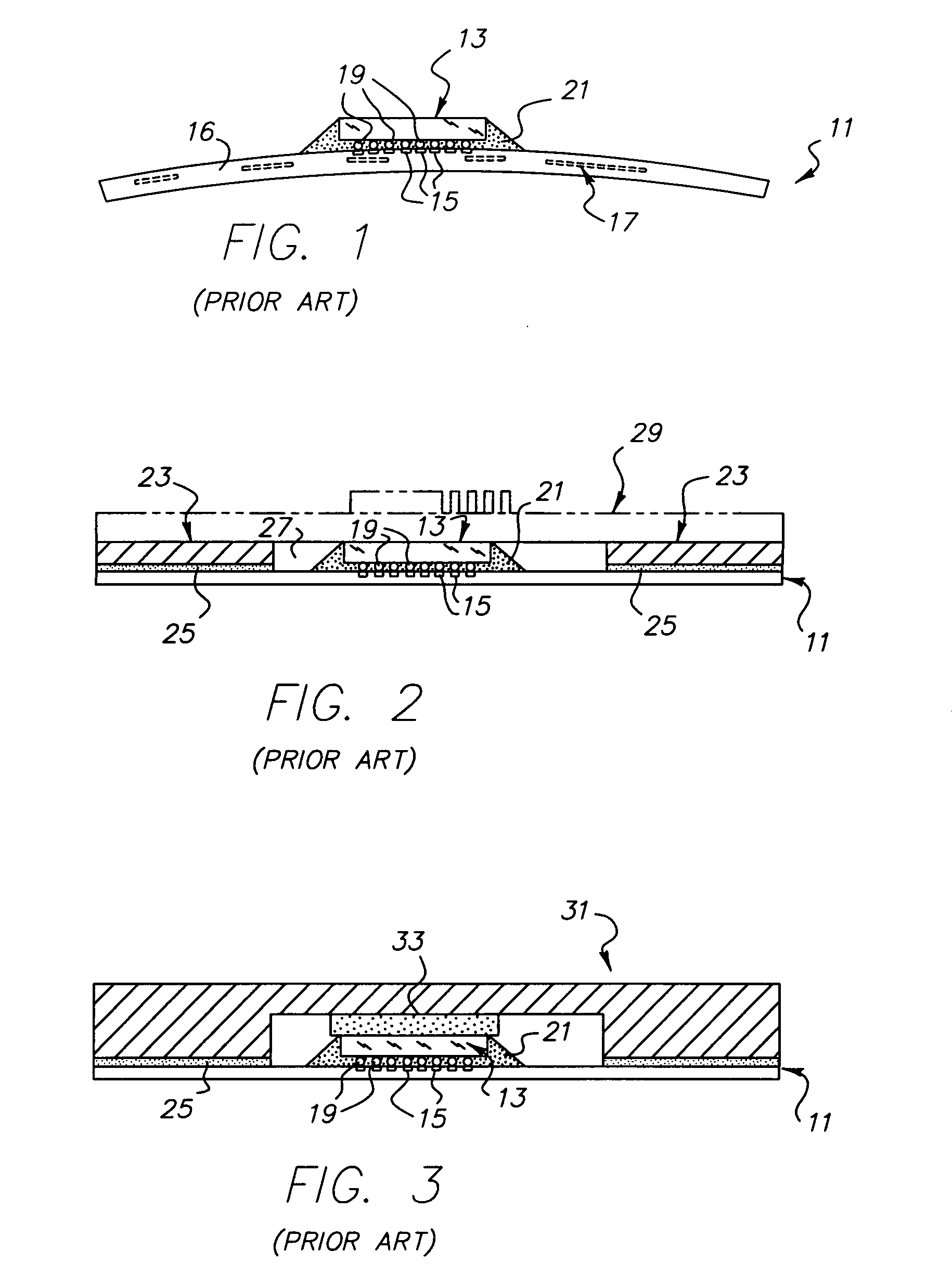
[0032]By the term “flexible circuit” or “flex circuit” as used herein is meant at least one thin dielectric layer of material having circuitry as part thereof. By the term “thin” is...


PUM


Abstract

A flexible circuit electronic package including a heat sink, a flexible circuit having a semiconductor chip positioned thereon and electrically coupled thereto, and a quantity of heat shrunk adhesive securing the flexible circuit to the heat sink such that the flexible circuit is planar. This package is then adapted for being positioned on and electrically coupled to a circuitized substrate such as a printed circuit board. A method of making this package is also provided.

Description

TECHNICAL FIELD[0001]This invention relates to electronic packages and particularly to such packages which include one or more flexible circuit members as part thereof.BACKGROUND OF THE INVENTION[0002]Flexible (or “flex”) circuit electronic packages typically include one or more flex circuit members each including at least one thin layer of dielectric (e.g., polyimide) with a pattern of conductors (e.g., copper pads) positioned on a surface thereof designed to accommodate a semiconductor chip (also referred to herein simply as a chip) thereon which is electrically connected to the conductors (e.g., using solder balls) and thereby to other circuitry of the flex circuit which is also coupled to the conductors. This flex circuit in turn is designed for being mounted on another circuitized substrate, typically in the form of a multilayered printed circuit board (also referred to herein simply as a PCB). The printed circuit board in turn typically includes a dielectric substrate (e.g., o...

Claims


Application Information

Patent Timeline
IPC IPC(8): H01L23/34
CPCH01L23/10H01L23/367H01L23/40H01L23/42H01L23/5387H01L2224/16H01L2224/73253H01L2924/01078H01L2924/01079H01L2924/09701H01L2924/01087H01L2224/73204H01L2224/16225H01L2224/32225H01L2924/00H01L2924/00011H01L2924/00014H01L2224/0401
Inventor ALCOE, DAVID J.CALMIDI, VARAPRASAD V.
Owner I3 ELECTRONICS
Why Eureka
Try Eureka