Image Processing Device

Active Publication Date: 2008-10-09
SONY CORP
View PDF14 Cites 17 Cited by
  • Summary
  • Abstract
  • Description
  • Claims
  • Application Information

AI Technical Summary

Benefits of technology

[0024]According to embodiments of the present invention, excellent advantages can be had in that occurrence o

Problems solved by technology

However, with the above-described related art, occurrence of false color can be reduced with images including high-frequency components with low color saturation, such as a stripe pattern of white and black, for example, but with cases of images with high-frequency component

Method used


Image

  • Image Processing Device
  • Image Processing Device
  • Image Processing Device

Examples


Example

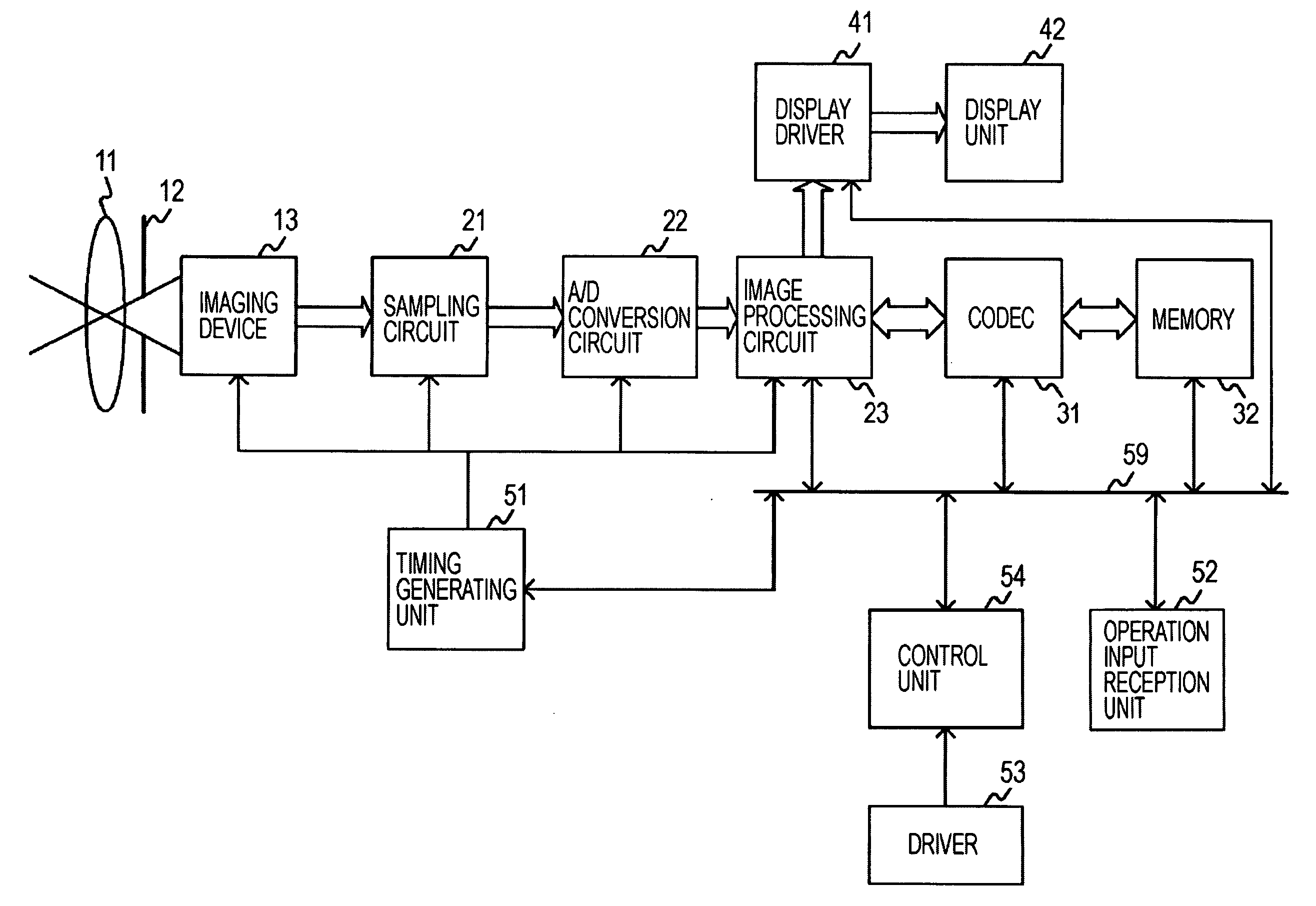
[0046]Embodiments of the present invention will be described in detail with reference to the drawings. FIG. 1 is a diagram illustrating an example of an imaging apparatus according to an embodiment of the present invention. The imaging apparatus is generally configured of an optical system, signal processing system, recording system, display system, and control system.

[0047]The optical system is configured of a lens 11 for converging a light image of a subject, an aperture 12 for adjusting the quantity of light of the light image, and an imaging device 13 for converting the converged light image into electrical signals by photoelectrical conversion. The imaging device 13 is realized by way of, for example, a CCD image sensor, CMOS image sensor, or the like.

[0048]The signal processing system is configured of a sampling circuit 21 for sampling electrical signals from the imaging device 13, an A / D conversion circuit 22 for converting analog signal supplied from the sampling circuit 21 ...


PUM


Abstract

An image processing device includes: an interpolation unit configured to perform interpolation along each of a plurality of directions in a neighbor region of a predetermined pixel of interest in an input image, and generate interpolation values for each; a chroma signal alias intensity calculating unit configured to calculate alias intensities of chroma signals from interpolation values of each of the plurality of directions from the interpolation unit; and a direction evaluation unit configured to generate evaluation values corresponding to each of the plurality of directions, based on the alias intensity of each of the chroma signals of the plurality of directions from the chroma signal alias intensity calculating unit.

Description

CROSS REFERENCES TO RELATED APPLICATIONS[0001]The present invention contains subject matter related to Japanese Patent Application JP 2007-098996 filed in the Japanese Patent Office on Apr. 5, 2007, the entire contents of which are incorporated herein by reference.BACKGROUND OF THE INVENTION[0002]1. Field of the Invention[0003]The present invention relates to an image processing device, and particularly to an image processing device for performing demosaicing processing of a mosaic image, and to a processing method thereof and a program for causing a computer to execute the same.[0004]2. Description of the Related Art[0005]Solid-state imaging devices such as CCD Charge Coupled Device) image sensors and CMOS (Complementary Metal Oxide Semiconductor) image sensors are normally configured with photoreceptors arrayed in a grid, with electric charges occurring due to photoelectric conversion at each photoreceptor being sequentially read out. Since a normal photoreceptor has a singular sp...

Claims


Application Information

Patent Timeline
IPC IPC(8): G06K9/32
CPCH04N9/045H04N23/843H04N25/134
Inventor YASUMA, FUMIHITOMITSUNAGA, TOMOO
Owner SONY CORP
Why Eureka
Try Eureka