Solid state image pickup device and its manufacture method

a solid-state image and pickup device technology, applied in the direction of semiconductor devices, basic electric elements, electrical appliances, etc., can solve the problems of likely blooming between pixels, suppress blooming between pixels, and suppress the effect of lowering the long wavelength sensitivity

Inactive Publication Date: 2008-10-09
FUJIFILM CORP
View PDF18 Cites 10 Cited by
  • Summary
  • Abstract
  • Description
  • Claims
  • Application Information

AI Technical Summary

Benefits of technology

[0024]An object of this invention is to provide a solid state image pickup device and its manufacture method capable of taking an image at a high quality.
[0026]This solid state image pickup device can take an image at a high quality by suppressing a long wavelength sensitivity from being lowered and suppressing blooming between pixels.
[0028]This manufacture method for a solid state image pickup device can manufacture a solid state image pickup device which can take an image at a high quality by suppressing a long wavelength sensitivity from being lowered and suppressing blooming between pixels.

Problems solved by technology

If the overflow barrier region 51 is formed at a deep position of the semiconductor substrate in order to retain the long wavelength light sensitivity, there arises a problem that blooming between pixels is likely to occur (e.g., refer to Japanese Patent Laid-open Publication No. 2000-150848).

Method used


Image

  • Solid state image pickup device and its manufacture method
  • Solid state image pickup device and its manufacture method
  • Solid state image pickup device and its manufacture method

Examples


first embodiment

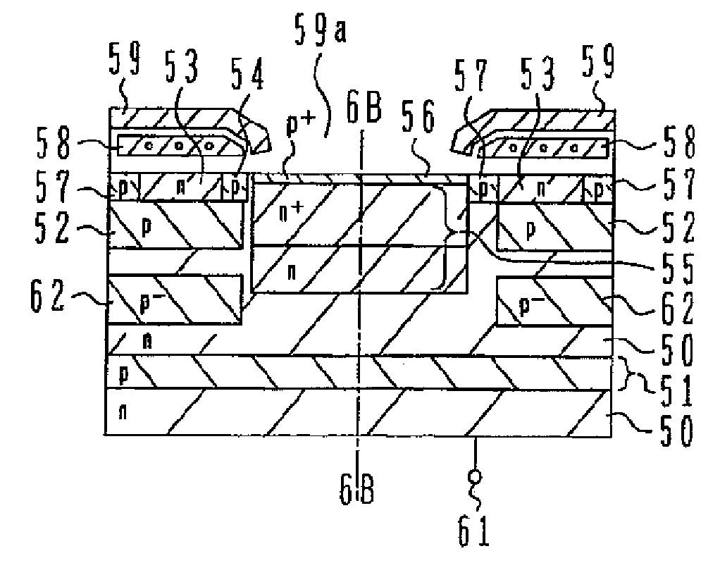
[0046]FIG. 2 is a schematic cross sectional view of a pixel area of a solid state image pickup device according to the

[0047]Although the structure of the solid state image pickup device is similar to that shown in FIG. 9B, it is different in that an overflow barrier region 51 is formed deeper in an n-type semiconductor substrate 50 and that a low concentration p-type (p−-type) impurity layer (pixel separation impurity layer) 62 is formed between a p-type impurity layer (channel protection impurity layer) 52 under the vertical transfer channel 53 and the overflow barrier region 51, e.g., at a middle depth between the layer 52 and region 51. The low concentration p-type (p−-type) impurity layer 62 is formed under the p-type impurity layer 52 and faces the p-type impurity layer 52.

[0048]The peak position of the p-type impurity concentration of the overflow barrier region 51 is at a depth of 3.5 μm from the substrate surface. The overflow barrier region 51 can be formed at this depth by...

second embodiment

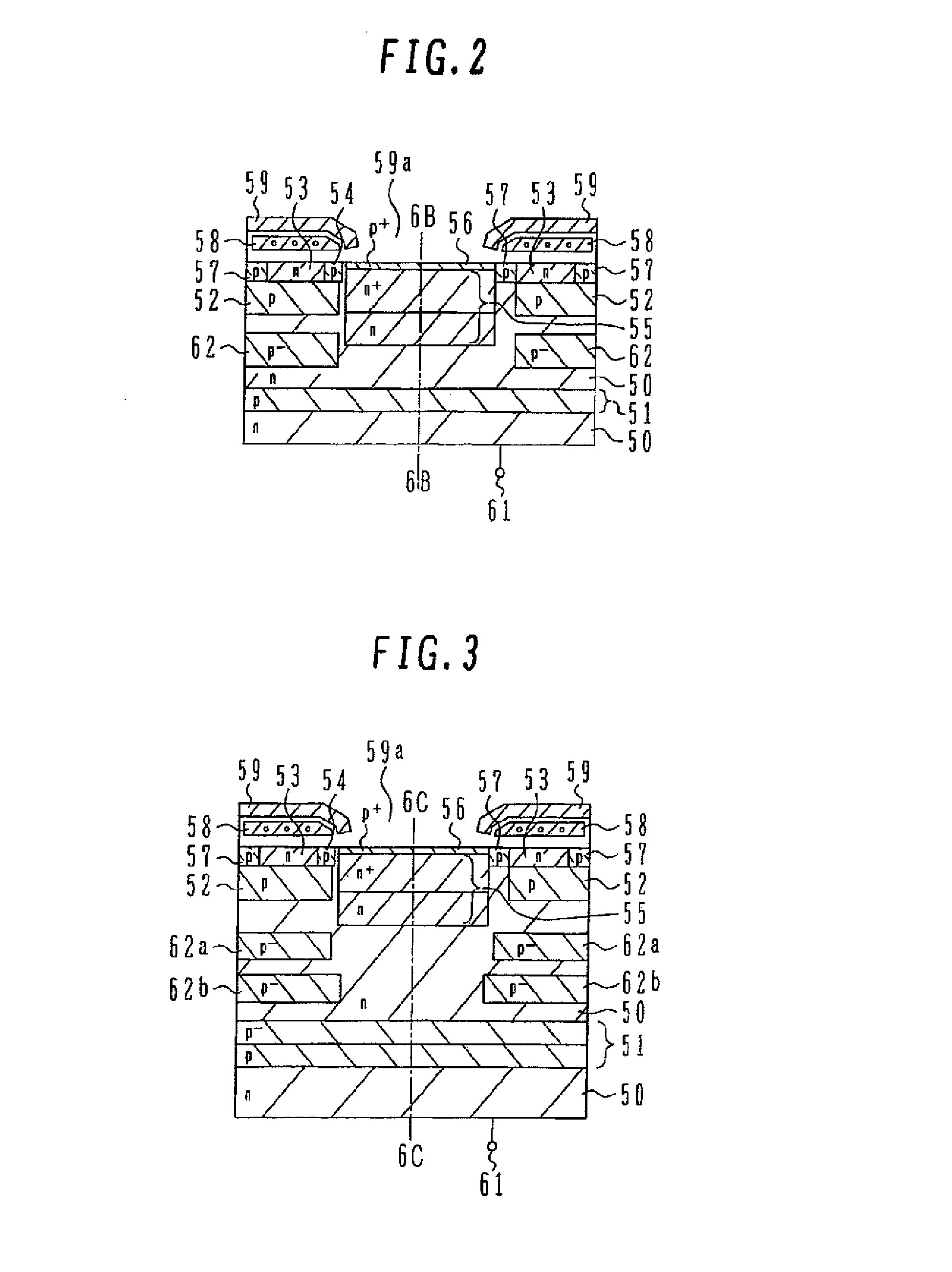
[0063]FIG. 3 is a schematic cross sectional view of a solid state image pickup device according to the

[0064]A first different point from the first embodiment shown in FIG. 2 is that an overflow barrier region has a multi-layer structure (in this example, two layers) along a substrate depth direction. In the first embodiment, the overflow barrier area 51 is made of only a single p-type impurity layer, whereas in the second embodiment, the overflow barrier region 51 is made of a p-type impurity layer and an upper p−-type impurity layer. A peak position of the p-type impurity concentration of the overflow barrier region 51 is at a depth of, e.g., 4.4 μm from the semiconductor substrate surface.

[0065]A preferable depth and effects of the peak position of the p-type impurity concentration of the overflow barrier region 51 are similar to the first embodiment. By making the overflow barrier region 51 have a multi-layer structure, an impurity concentration of the p-side region of a pn junct...


PUM


Abstract

A solid state image pickup device is provided which includes: charge accumulation regions disposed in a semiconductor substrate in a matrix shape; a plurality of vertical transfer channels formed in the semiconductor substrate each in a close proximity to each column of the charge accumulation regions; vertical transfer electrodes formed above the vertical transfer channels; a channel protective impurity layer formed just under the vertical transfer channel and surrounding the charge accumulation region; one or more pixel separation impurity layers formed under the channel protective impurity layer and at a position facing the channel protective impurity layer; an overflow barrier region having a peak position of an impurity concentration at a position deeper than the pixel separation impurity layer, the peak position of the impurity concentration being at a depth of 3 μm or deeper from a surface of the semiconductor substrate; and a horizontal CCD for transferring signal charges transferred from the vertical transfer channels in a horizontal direction.

Description

CROSS REFERENCE TO RELATED APPLICATION[0001]This application is a Divisional of co-pending application Ser. No. 11 / 188,646 filed on Jul. 26, 2005, and for which priority is claimed under 35 U.S.C. §120; and this application claims priority of Application No. 2004-255530 filed in Japan on Sep. 2, 2004 under 35 U.S.C. §119; the entire contents of all are hereby incorporated by reference.BACKGROUND OF THE INVENTION[0002]A) Field of the Invention[0003]The present invention relates to a solid state image pickup device having an overflow barrier region and its manufacture method.[0004]B) Description of the Related Art[0005]FIG. 8 is a schematic plan view of a pixel area of a solid state image pickup device.[0006]The pixel area is constituted of a plurality of photoelectric conversion elements 60, vertical transfer channels 53, vertical transfer electrodes (first layer vertical transfer electrodes 58a and second layer vertical transfer electrodes 58b) and element isolation regions 57.[0007...

Claims


Application Information

Patent Timeline
Patent Type & Authority Applications(United States)
IPC IPC(8): H01L21/265H01L31/18
CPCH01L27/14887
Inventor NOMURA, YUKOUYA, SHINJI
Owner FUJIFILM CORP
Why Eureka
Try Eureka