Semiconductor Switch with Integrated Delay Circuit

a technology of delay circuit and semiconductor, applied in the direction of mechanical equipment, electrical equipment, engine ignition, etc., can solve the problems of high-current load pwm control, large number of components, high cost, special software for microcontrollers which is an expensive component, etc., to improve the pwm control of multi-stage electric loads.

Inactive Publication Date: 2008-10-30
CATEM DEVELEC
View PDF4 Cites 5 Cited by
  • Summary
  • Abstract
  • Description
  • Claims
  • Application Information

AI Technical Summary

Benefits of technology

[0015]It is therefore the object of the present invention to provide an improved circuit for generating the phase-shifted PWM signals. Another object of the present invention is to provide an integrated semiconductor switch on the basis of which the circuit for

Problems solved by technology

A PMW control of high-current loads, in particular of high-current loads in a vehicle electrical system, such as an electric auxiliary heating system or the glow plugs of an Diesel engine, is disadvantageous with regard to the load peaks which occur due to the clocking and which may become noticeable e.g. by an unpleasant flickering of the passenger compartment illumination, and with regard to the EMC problems (EMC: electromagnetic compatibility) entailed by the switching processes.
A disadvantage of the generation of signals for a phase-shifted control of a plurality of load circuits by means of a microcontroller is the comparatively large number of components required and the resultant costs as well as the space required by th

Method used


Image

  • Semiconductor Switch with Integrated Delay Circuit
  • Semiconductor Switch with Integrated Delay Circuit
  • Semiconductor Switch with Integrated Delay Circuit

Examples


Embodiment Construction

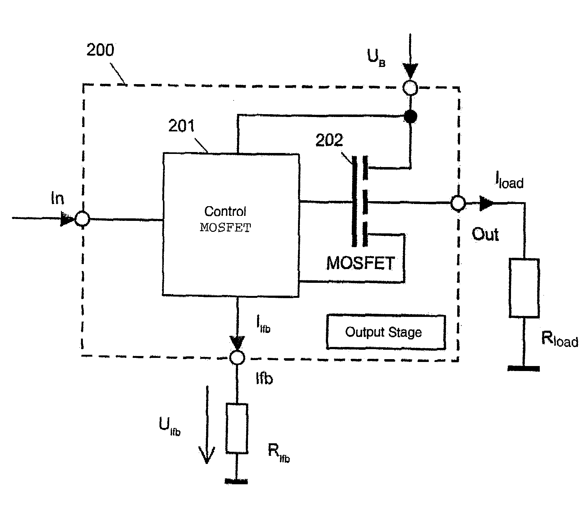
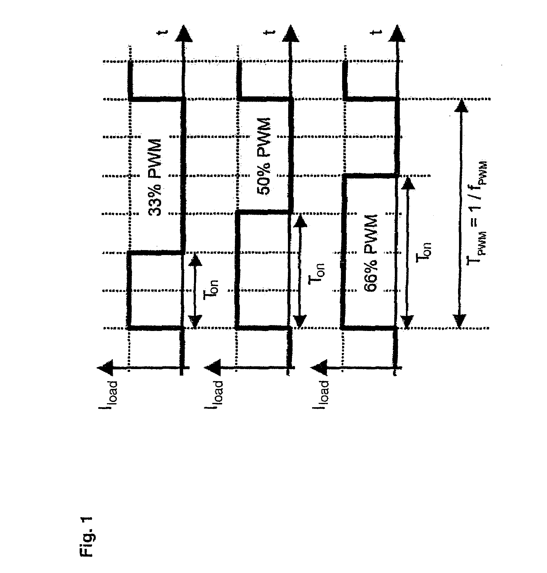
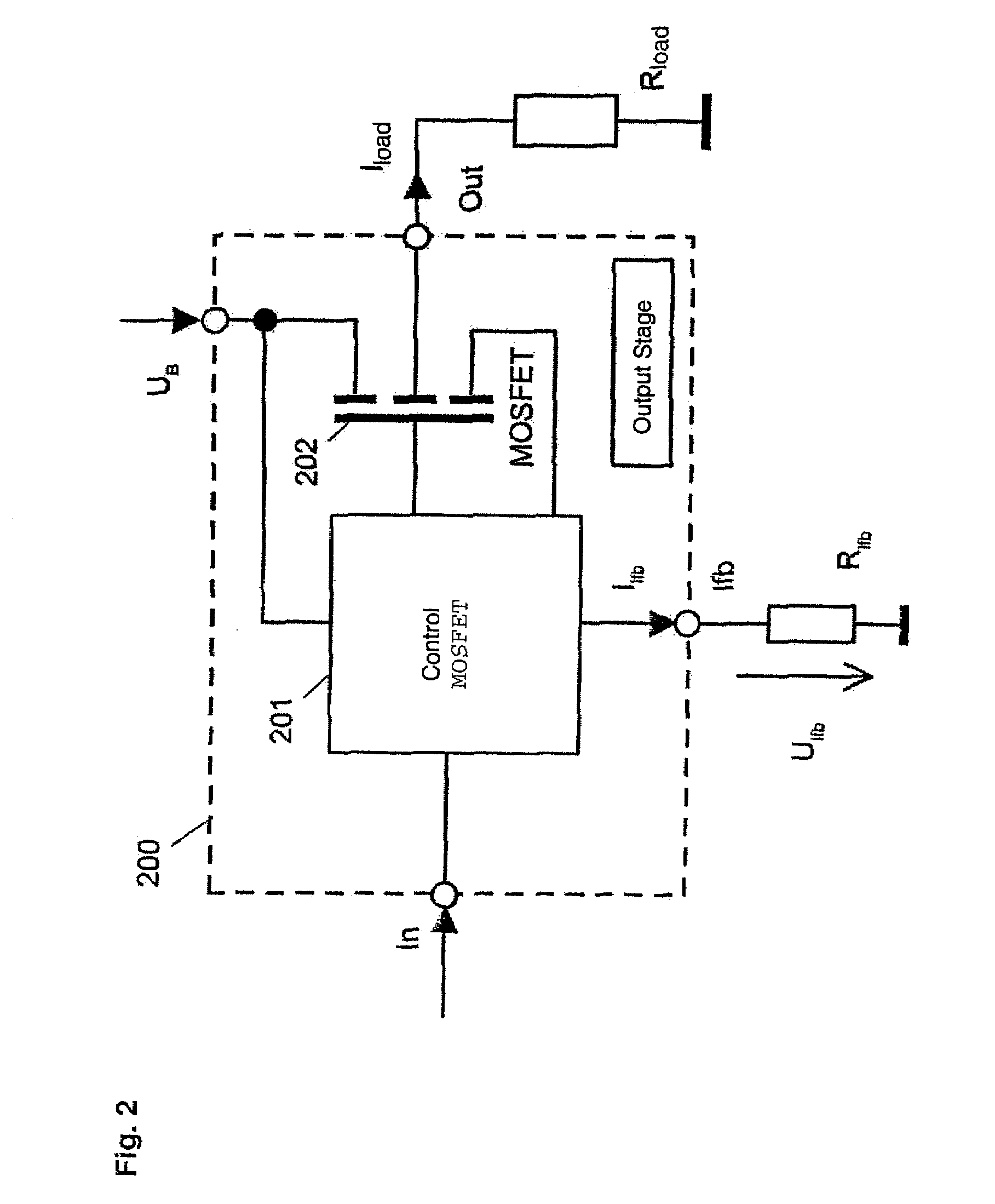
[0039]FIG. 6A shows an output stage for PWM control of a load according to an embodiment of the present invention. The load Rload is connected to the supply voltage UB through a power semi-conductor switch 602, preferably a MOSFET. The load current lload is modulated by the control circuit 601 in accordance with the external PWM signal PWMin. The control circuit 601 can execute additional monitoring functions and protect the power semiconductor switch 602 against overload. The control circuit 601 can e.g. monitor the temperature of the power semi-conductor switch 602 and / or the switched current. If predetermined limit values are exceeded, the control circuit can switch off the semiconductor switch. In addition, a feedback signal llfb, used as a measure for the load current lload detected by a current sensor, can be provided at a terminal lfb for an extended external control.

[0040]The output stage according to the present invention is additionally provided with a PWM delay circuit 60...


PUM


Abstract

For controlling a multi-stage load with pulsewidth modulation (PWM), the individual stages have normally separately applied thereto load currents which are clocked in a phase-shifted mode so as to avoid load peaks. An output stage for PWM control of a load stage with a delay circuit which, in addition to the load current modulated by a PWM input signal, supplies a PWM output signal that is delayed by a predetermined fraction of the period duration relative to the PWM input signal. The output stage can especially be realized by integrating the delay circuit together with the actual power semiconductor switch and an associated monitoring and control circuit in a single component. By cascading such output stages, a controller for phase-shifted PWM control of multi-stage loads, which is independent of a precise time base, can be realized in a simple manner.

Description

BACKGROUND OF THE INVENTION[0001]1. Field of the Invention[0002]The present invention relates to a semiconductor switch with an integrated delay circuit, a controller for pulsewidth-modulated control of a multistage electric load and to a corresponding method.[0003]2. Description of the Related Art[0004]The control of the power consumption of an electric load, such as e.g. electric heatings, filament lamps, DC motors, etc., can be effected in a conventional manner through pulsewidth modulation (PWM). The supply voltage is in this case switched on and off at periodic intervals. The power consumption of the load can be controlled continuously via the duty cycle, i.e. the ratio of the on-time Ton within a period to the period duration TPWM (cf. FIG. 1). The on-time Ton=0 represents the OFF state, the on-time Ton=TPWM means constantly ON, i.e. maximum power. In comparison with a linear control of the supply voltage or of the current, e.g. by means of a series transistor, the power losse...

Claims


Application Information

Patent Timeline
IPC IPC(8): H03K7/08
CPCH03K17/08H03K17/162H03K17/284H03K17/687F02P19/023H03K7/08
Inventor UHL, GUNTERWANDRES, STEFFEN
Owner CATEM DEVELEC
Why Eureka
Try Eureka