Eureka AIR delivers breakthrough ideas for toughest innovation challenges, trusted by R&D personnel around the world.

Method of Manufacturing Electrical Conductors for a Semiconductor Device

a manufacturing method and technology for semiconductor devices, applied in semiconductor devices, semiconductor/solid-state device details, electrical apparatus, etc., can solve the problems of increasing the difficulty of creating vias and filling them with conductive materials, stress on conductive materials, and high cost of patterning after dicing, so as to avoid weakening or distortion of semiconductor wafers or overall devices, the effect of simplifying the plating process

Inactive Publication Date: 2008-12-04
INFINEON TECH AG
View PDF10 Cites 3 Cited by
  • Summary
  • Abstract
  • Description
  • Claims
  • Application Information

AI Technical Summary

Benefits of technology

[0014]The invention seeks to solve the above problems by making vertical conductors through one or more deep etched channels or openings in a wafer or layer of a semiconductor device, which allow electrical interconnection between two sides of the semiconductor wafer or layer. Each channel defines a gap that extends between the surfaces of the two sides of the semiconductor wafer. An electrical conductor is then formed on a wall of the channel by patterning conductive material on an insulating layer, while the gap between the semiconductor wafer or layer surfaces is maintained. Such a gap is advantageous as it effectively acts as a buffer, allowing for a difference in the thermal expansion properties of the semiconductor, insulator and conductor materials. There is therefore no weakening or distortion of the semiconductor wafer or the overall device when a change in temperature occurs. Additionally, each channel is wide enough to simplify the plating process and thus provide multiple conductors through the channels. The channels are preferably placed along the sawing lines of the semiconductor wafer. In this way the conductors can occupy a minimum of the active wafer area, without weakening the die.

Problems solved by technology

However, there are many disadvantages associated with the known techniques.
Patterning after dicing is expensive in high volumes, while creating vias and filling them with conductive material is increasingly technically difficult with thicker semiconductor wafers.
The thermal expansion of the conductive material is often mismatched compared to that of the semiconductor wafer, and hence the conductive material induces stress in the semiconductor wafer.

Method used


Image

  • Method of Manufacturing Electrical Conductors for a Semiconductor Device
  • Method of Manufacturing Electrical Conductors for a Semiconductor Device
  • Method of Manufacturing Electrical Conductors for a Semiconductor Device

Examples


Embodiment Construction

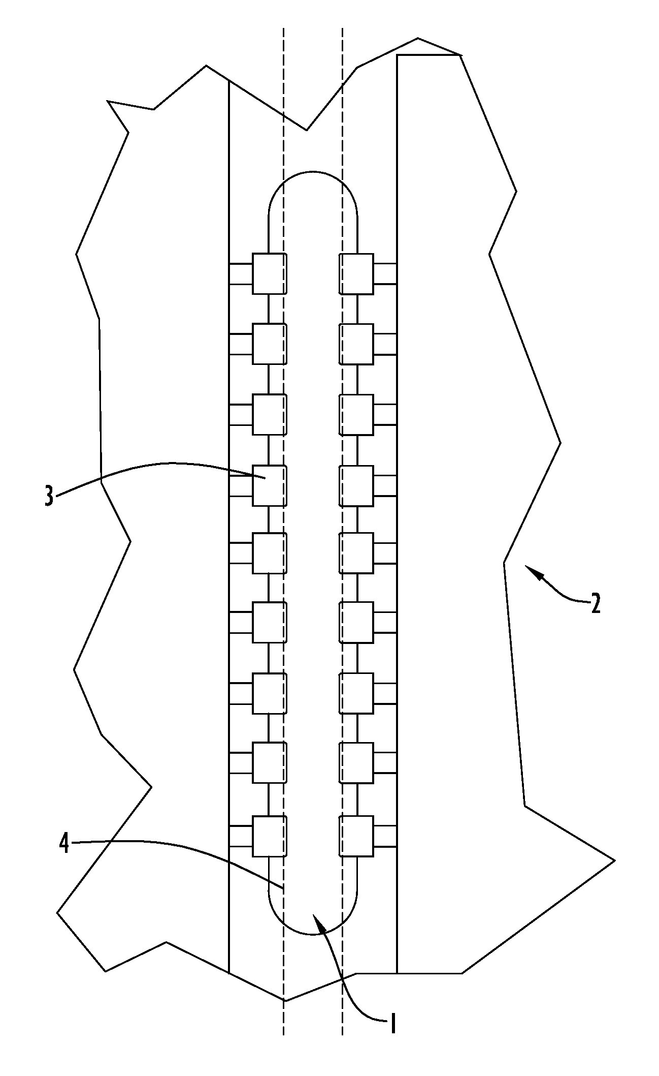
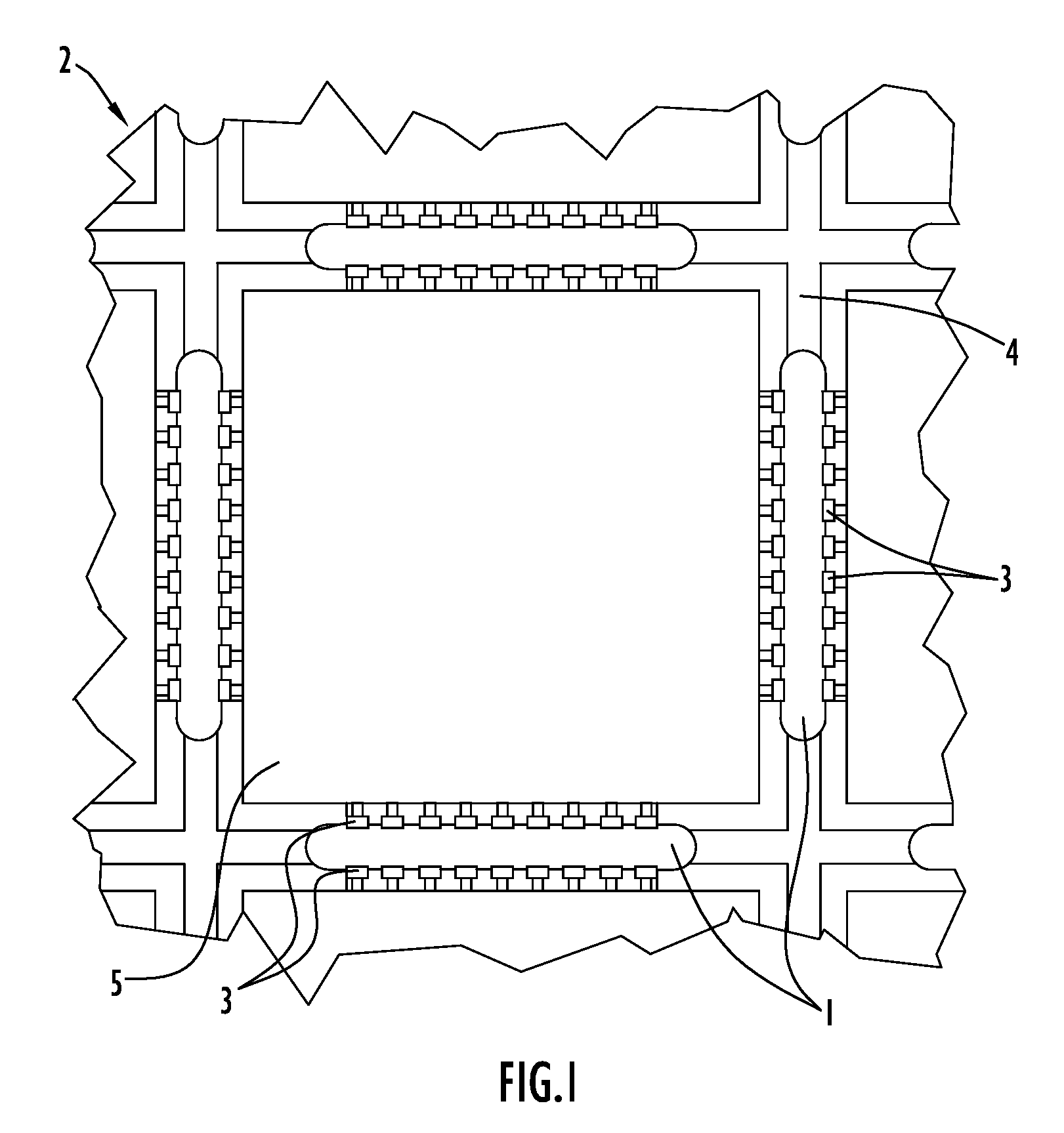
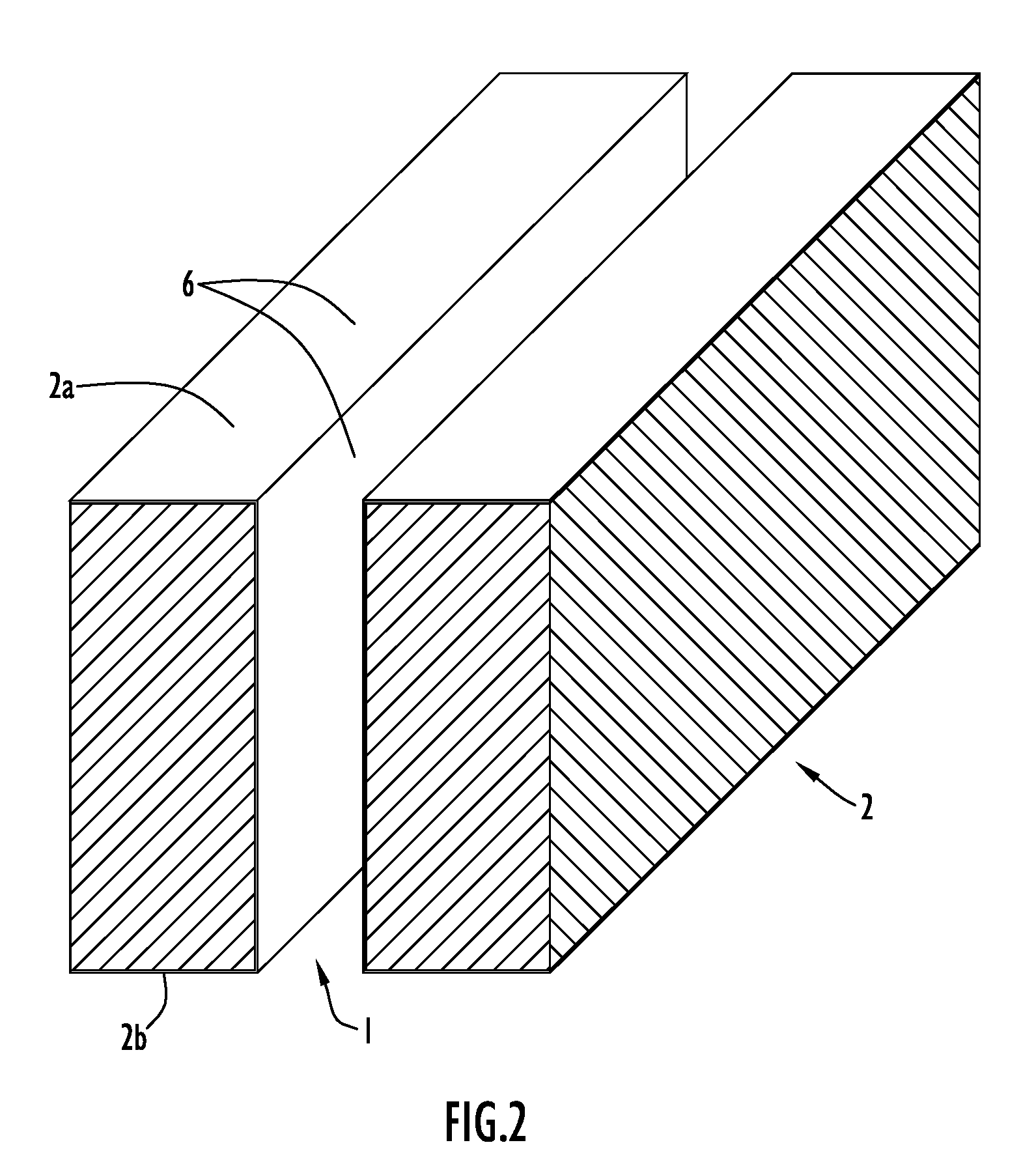
[0022]Referring to an embodiment of the invention shown in FIG. 1, one or more channels or openings 1 are created between two surfaces 2a and 2b (not shown, see FIG. 2) of a semiconductor wafer or layer 2, and multiple electrically conductive elements 3 are provided between the surfaces 2a and 2b to allow for electrical connection therebetween. A gap between the semiconductor wafer or layer surfaces is maintained. Such a gap is advantageous as it allows for a difference in the thermal expansion properties of the semiconductor, insulator and conductor materials. There is therefore no weakening or distortion of the semiconductor wafer or the overall device when a change in temperature occurs.

[0023]The channels 1 are preferably placed along the sawing gates 4 of the semiconductor wafer 2 as shown in FIG. 1. In this way, openings that are large enough to simplify the processes needed to make vertical conductors 3 between layers of a semiconductor device incorporating the semiconductor w...


PUM


Abstract

A method of manufacturing an electrical conductor for a semiconductor device having one or more layers includes etching from a first surface to a second surface of at least one layer of the device to form a channel having a wall extending from the first surface to the second surface. The channel defines a gap extending from the first surface to the second surface. An insulating layer is provided on the channel wall. Conductive material is patterned on the channel wall to form multiple separate electrical conductors, which are insulated from material of the at least one layer by the insulating layer, thereon, such that the gap that extends from the first surface to the second surface is maintained. A corresponding semiconductor device is also provided.

Description

CROSS REFERENCE TO RELATED APPLICATIONS[0001]This application claims priority under 35 U.S.C. §119 to Application No. EP07109351.2 filed on May 31, 2007, entitled “Method of Manufacturing Electrical Conductors for a Semiconductor Device,” the entire contents of which are hereby incorporated by reference.FIELD OF THE INVENTION[0002]The present invention relates to a method of manufacturing electrical conductors for a semiconductor device.BACKGROUND[0003]Various methods are known in which electrical elements are provided between two sides of a wafer, for example a semiconductor wafer, in order to allow electrical connection between the layers of a device or to external components connected to the device.[0004]Known techniques involve either patterning edges of a semiconductor wafer after dicing or creating vias or channels through a layer of semiconductor material semiconductor wafer and filling the vias with electrically conductive material, each via providing a single electrical con...

Claims


Application Information

Patent Timeline
Patent Type & Authority Applications(United States)
IPC IPC(8): H01L21/768H01L23/538
CPCB81B2207/07B81C1/00095H01L2924/1461H01L2924/00014H01L2924/01006H01L21/76898H01L23/481H01L24/03H01L24/05H01L24/24H01L24/73H01L24/82H01L24/94H01L24/95H01L25/0657H01L25/50H01L2224/05599H01L2224/18H01L2225/06551H01L2924/01033H01L2924/01078H01L2924/00
Inventor SKOG, TERJENILSEN, SVEIN MOLLER
Owner INFINEON TECH AG
Why Eureka
Eureka Blog
Learn More