Eureka AIR delivers breakthrough ideas for toughest innovation challenges, trusted by R&D personnel around the world.

Fill plated structure of inner via hole and manufacturing method thereof

Inactive Publication Date: 2006-07-06
SAMSUNG ELECTRO MECHANICS CO LTD
View PDF6 Cites 36 Cited by
  • Summary
  • Abstract
  • Description
  • Claims
  • Application Information

AI Technical Summary

Benefits of technology

[0033] Another object of the present invention is to provide a method of manufacturing a fill plated structure of an inner via hole, which is advantageous because a plating process is simplified.

Problems solved by technology

Similarly, lots of ICs (Integrated Circuits) having superb performance and various electronic components would be useless, too, if they were aimlessly gathered.
Further, since heat generated from chips upon operation of the mounted components may damage the chips, designs for radiating portions of the substrate required to rapidly remove the generated heat so as to protect the chips from the heat must be provided.
The reason why the electroless plating process precedes the copper electroplating process is that an inner wall of the drilled hole is formed of an insulating material, and copper electroplating by electrolysis cannot be performed thereon.
In addition, since the electroless plated film, which is undesirably thin and has insufficient properties, cannot be used as it is, it should be further plated by the copper electroplating process.
As mentioned above, the process of filling the inner via hole with the ink is disadvantageous because heat conductivity of the substrate is limited due to the ink, and also, the subsequent cap plating process is further required on upper and lower portions of the inner via hole filled with the ink.
Thus, the above process becomes complicated.
As mentioned above, the process of fill plating the blind via hole is disadvantageous because the blind via hole has an exposed upper portion, unlike the inner via hole, and thus, limitations are imposed on the plating growth depth of the via hole upon fill plating.

Method used


Image

  • Fill plated structure of inner via hole and manufacturing method thereof
  • Fill plated structure of inner via hole and manufacturing method thereof
  • Fill plated structure of inner via hole and manufacturing method thereof

Examples


Embodiment Construction

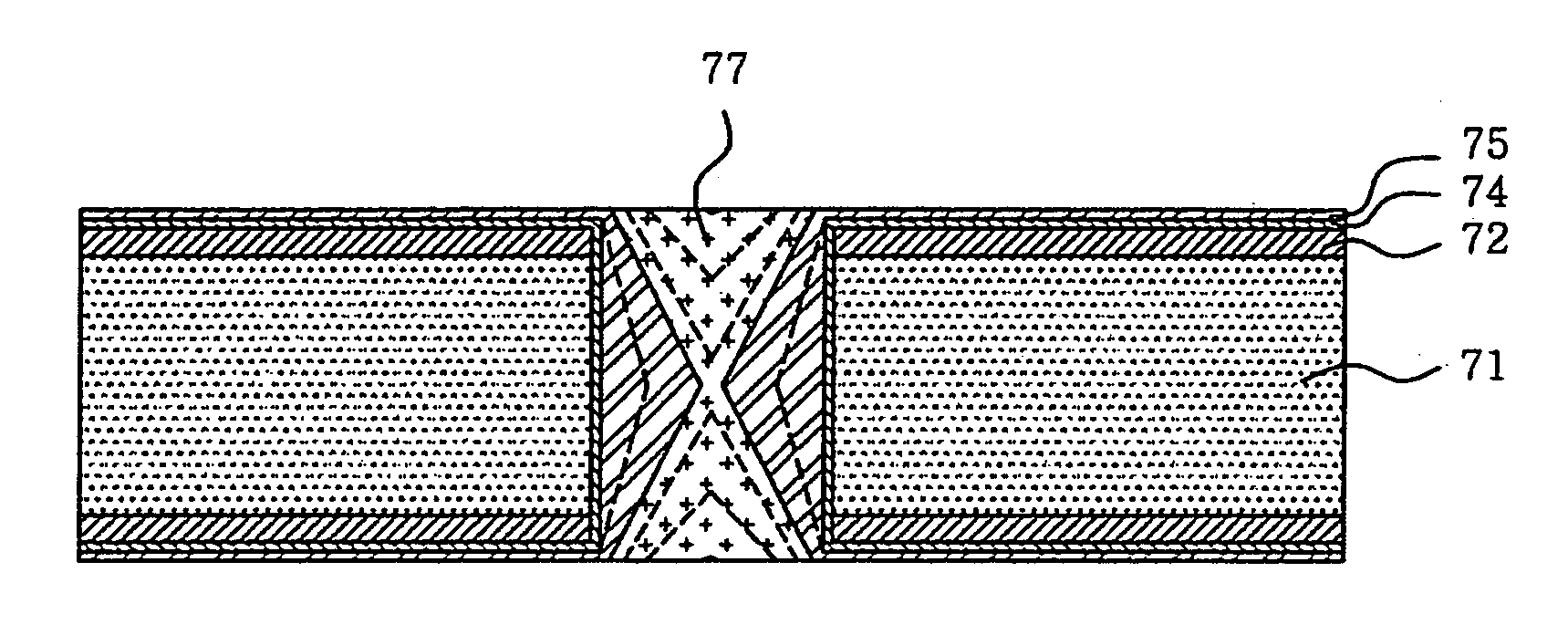
[0048] Hereinafter, a detailed description will be given of a fill plated structure of an inner via hole and a method of manufacturing the same according to the present invention, with reference to the appended drawings.

[0049]FIG. 6 shows a fill plated structure of an inner via hole, according to an embodiment of the present invention.

[0050] The fill plated structure of the inner via hole includes an electroless plated layer 63 formed on a CCL having an inner via hole for interlayer connection, a first copper electroplated layer 64 formed on the electroless plated layer 63, and a second copper electroplated layer 65 formed on the first copper electroplated layer 64.

[0051] That is, the electroless plated layer 63 is obtained by forming the inner via hole for interlayer electrical connection through the CCL having an insulating layer 61 and copper foil layers 62 formed on both surfaces thereof, and plating upper surfaces of the copper foil layers 62 and an inner wall of the via hol...


PUM

PropertyMeasurementUnit
Densityaaaaaaaaaa
Densityaaaaaaaaaa
Densityaaaaaaaaaa

Abstract

A fill plated structure of an inner via hole, which includes an electroless plated layer formed on a copper clad laminate having an inner via hole formed therethrough, a first copper electroplated layer formed on the electroless plated layer on the copper clad laminate and formed on an inner wall of the via hole to form an belly portion having a belly shape, and a second copper electroplated layer formed on the first copper electroplated layer of a surface of the copper clad laminate and formed on upper and lower portions of the first copper electroplated layer of the inner wall of the via hole to fill the via hole; and a method of manufacturing the same.

Description

INCORPORATION BY REFERENCE [0001] The present application claims priority under 35 U.S.C. §119 to Korean Patent Application No. 2004-116801 filed on Dec. 30, 2004. The content of the application is incorporated herein by reference in its entirety. BACKGROUND OF THE INVENTION [0002] 1. Field of the Invention [0003] The present invention relates, generally, to a fill plated structure of an inner via hole and a manufacturing method thereof. More particularly, the present invention relates to a fill plated structure of an inner via hole, in which a first plated layer is formed in a belly shape on an inner wall of the via hole using a pulse-reverse plating process, and then reverse current is transformed to form a second plated layer on upper and lower portions of the first plated layer of the inner wall of the via hole so as to fill the via hole; and a method of manufacturing the same. [0004] 2. Description of the Related Art [0005] Were it not for software, a computer would be nothing ...

Claims


Application Information

Patent Timeline
IPC IPC(8): H05K1/11H01K3/10
CPCH05K3/423H05K3/427H05K2201/09563H05K2203/1476Y10T29/49126H01L2924/0002H05K2203/1492Y10T29/49165H01L2924/00H05K1/11
Inventor SONG, CHANG KYUKIM, TAE HOONKIM, KYUNG O.LEE, WOO YOUNGMOK, JEE SOO
Owner SAMSUNG ELECTRO MECHANICS CO LTD
Why Eureka
Eureka Blog
Learn More