Image processing apparatus and image processing method

a technology of image processing apparatus and image processing method, which is applied in the field of defectivepixelcorrection technology, can solve the problems of increased noise, defective pixels, abnormal image signals,

Inactive Publication Date: 2008-12-04
CANON KK
View PDF7 Cites 13 Cited by
  • Summary
  • Abstract
  • Description
  • Claims
  • Application Information

AI Technical Summary

Benefits of technology

[0022]According to an aspect of the present invention, an image processing apparatus is provided, which includes a storage medium in which first correction data is stored in advance, a generator circuit arranged to generate second correction data using image data that is read from an image-pickup device in which charge accumulation is performed in a state in which the image-pickup device is shielded from light, a first correction circuit arranged to correct image data associated with a defective pixel of the image-pickup device on the basis of the first correction data, a second correction circuit arranged to correct image data associated with a defective pixel of the image-pickup device on the basis of the second correction data, and a control circuit operable to select either the first correction circuit or the second correction circuit for correcting image data associated with a defective pixel of the image-pickup device based on the number of pixels in image data read from the image-pickup device.
[0023]According to another aspect of the present invention, an image processing apparatus is provided, which includes a storage medium in which first correction data is stored in advance, a generator circuit arranged to generate second correction data using image data that is read from an image-pickup device in which charge accumulation is performed in a state in which the image-pickup device is shielded from light, a first correction circuit arranged to correct image data associated with a defective pixel of the image-pickup device on the basis of the first correction data, a second correction circuit arranged to correct image data associated with a defective pixel of the image-pickup device on the basis of the second correction data, and a control circuit arranged to select the first correction circuit or the second correction circuit for correcting image data associated with a defective pixel of the image-pickup device on the basis of whether image data read from the image-pickup device corresponds to a moving image or a still image.

Problems solved by technology

In the related art, it has been known that, in a solid-state image-pickup device, such as a charge-coupled device (CCD) sensor and a complementary metal-oxide-semiconductor (CMOS) sensor, defective pixels, which output abnormal image signals, occur in the manufacturing process of the solid-state image-pickup device.
It is very difficult to completely avoid the occurrence of the defective pixels in the manufacturing process of the solid-state image-pickup device.
When the thinned-out reading process is simply performed, the sampling frequency is spatially reduced, resulting in an increase in noise.
Furthermore, there are the following problems.
However, address re-conversion is performed for each reading method using firmware of the camera, the load of a conversion process is heavy.
Accordingly, because plenty of time is necessary to perform the conversion process, it is very difficult to finish the conversion process in a realistically short time.
The data size of the defect-correction data is significantly large.
Accordingly, the performance of the address conversion needs more complicated processing.
Thus, various factors responsible for the increase in cost, for example, one of which is the increase in test time in the manufacturing process, occur.

Method used


Image

  • Image processing apparatus and image processing method
  • Image processing apparatus and image processing method
  • Image processing apparatus and image processing method

Examples


Embodiment Construction

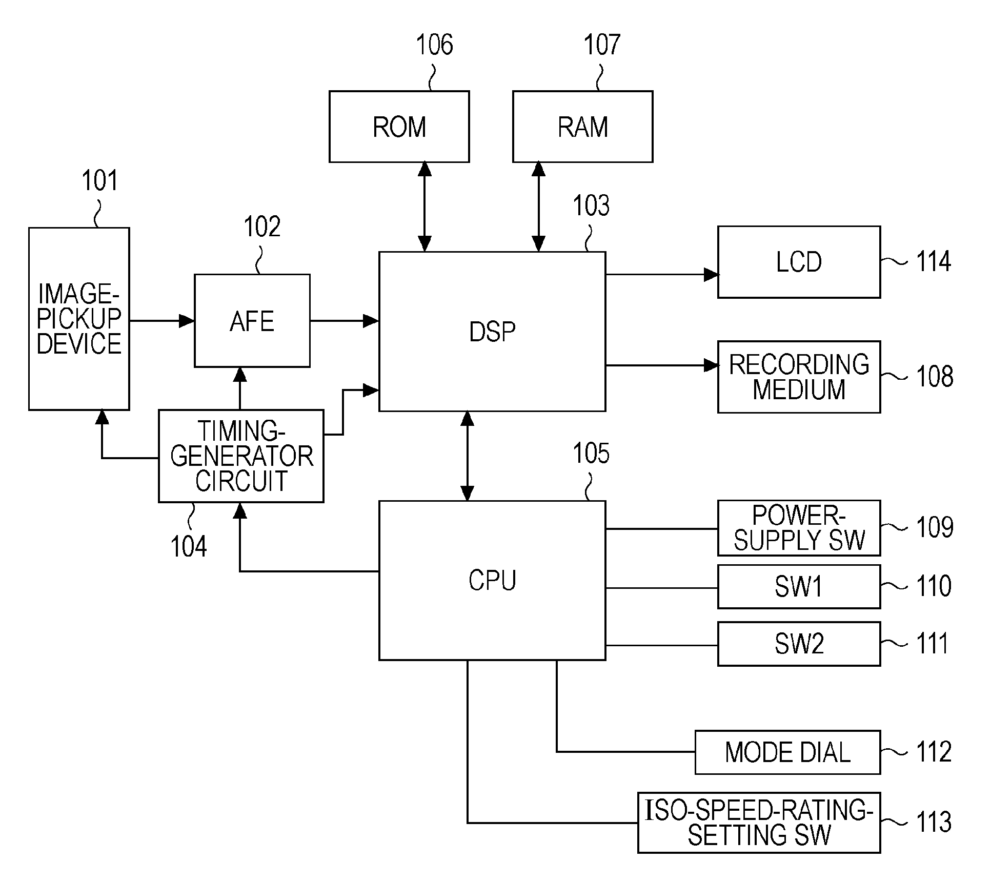
[0039]Exemplary embodiments of the present invention will now be described with reference to the accompanying drawings. FIG. 1 is a schematic block diagram of a configuration of an image-pickup apparatus that is an image processing apparatus according to an embodiment of the present invention.

[0040]The image-pickup apparatus includes an image-pickup device 101, an analog front end (AFE) 102, a digital signal processor (DSP) 103, a timing-generator circuit 104, and a central processing unit (CPU) 105.

[0041]As the image-pickup device 101, for example, a CMOS sensor (a solid-state image-pickup device) is used.

[0042]The CMOS sensor includes an amplifier circuit (not shown) that is capable of switching gains on the basis of ISO speed ratings. Image data including an image that is picked up by the CMOS sensor can be read in an all-pixel reading mode (in a first operation mode), in which image data is read from all pixels, a thinned-out reading mode (in a second operation mode), in which i...


PUM


Abstract

When pixel data of a solid-state image-pickup device is read in various types of methods to pick up images, a correction process for defective pixels is easily performed at a low cost. As defect-correction data in a case in which a still image is shot, data is used, which is acquired when an image-pickup device is shipped from a manufacturing factory. In a case of an operation in a reading mode for a moving image, immediately before a reading operation is performed, charge is accumulated in a state in which the image-pickup device is shielded from light, and image data is read. Addresses of defective pixels to be corrected are detected from the image data, and stored in a RAM as the defect-correction data. When a moving image is shot, a defect-correction process is performed using the data.

Description

BACKGROUND OF THE INVENTION[0001]1. Field of the Invention[0002]The present invention relates to a defective-pixel-correction technology in which image signals associated with defective pixels that have occurred in a solid-state image-pickup device are corrected.[0003]2. Description of the Related Art[0004]In the related art, it has been known that, in a solid-state image-pickup device, such as a charge-coupled device (CCD) sensor and a complementary metal-oxide-semiconductor (CMOS) sensor, defective pixels, which output abnormal image signals, occur in the manufacturing process of the solid-state image-pickup device. It is very difficult to completely avoid the occurrence of the defective pixels in the manufacturing process of the solid-state image-pickup device. Accordingly, in the related art, a defective-pixel-correction technology has been realized, in which image signals output from defective pixels are corrected using image processing.[0005]In a defective-pixel-correction met...

Claims


Application Information

Patent Timeline
Patent Type & Authority Applications(United States)
IPC IPC(8): H04N9/64H04N5/343H04N5/345H04N5/367
CPCH04N5/23245H04N5/343H04N5/345H04N5/367H04N23/667H04N25/42H04N25/44H04N25/68
Inventor KITANI, KAZUNARI
Owner CANON KK
Why Eureka
Try Eureka