Memory cell that employs a selectively deposited reversible resistance-switching element and methods of forming the same

a memory cell and reversible resistance technology, applied in the field of nonvolatile memories, can solve the problems of difficult fabrication of memory devices from rewriteable resistivity-switching materials

Active Publication Date: 2009-01-01
SANDISK TECH LLC
View PDF99 Cites 186 Cited by
  • Summary
  • Abstract
  • Description
  • Claims
  • Application Information

AI Technical Summary

Benefits of technology

[0008]In a first aspect of the invention, a method of forming a memory cell is provided that includes (1) forming a steering element above a substrate; and (2) forming a reversible resistance-switching element coupled to the steering element using a selective deposition process.

Problems solved by technology

However, fabricating memory devices from rewriteable resistivity-switching materials is difficult; and improved methods of forming memory devices that employ resistivity-switching materials are desirable.

Method used


Image

  • Memory cell that employs a selectively deposited reversible resistance-switching element and methods of forming the same
  • Memory cell that employs a selectively deposited reversible resistance-switching element and methods of forming the same
  • Memory cell that employs a selectively deposited reversible resistance-switching element and methods of forming the same

Examples


first exemplary embodiment

OF A MEMORY CELL

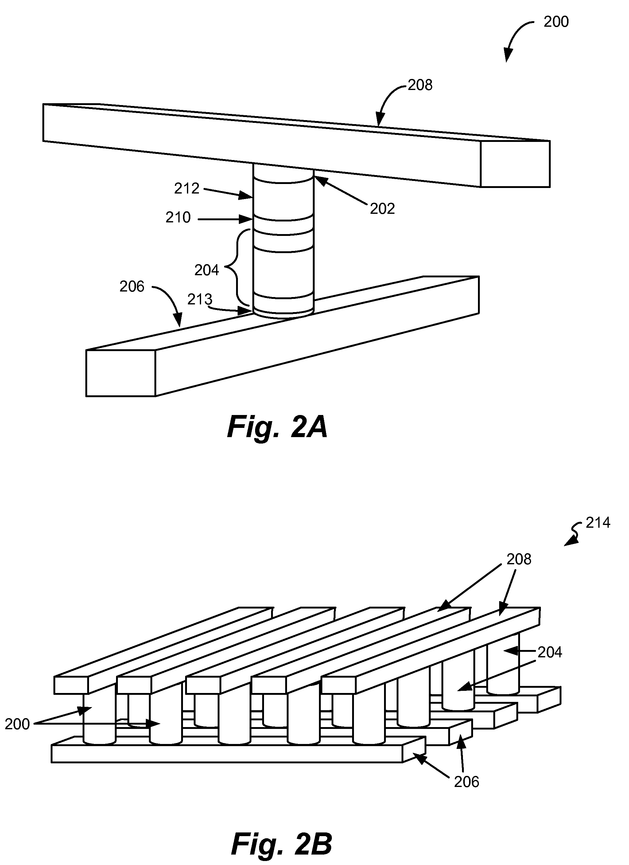
[0039]FIG. 2A is a simplified perspective view of a first embodiment of a memory cell 200 provided in accordance with the present invention. With reference to FIG. 2A, the memory cell 200 includes a reversible resistance-switching element 202 coupled in series with a diode 204 between a first conductor 206 and a second conductor 208. In some embodiments, a barrier layer 210 and / or a conductive layer 212 may be formed between the reversible resistance-switching element 202 and the diode 204. For example, the barrier layer 210 may include titanium nitride, tantalum nitride, tungsten nitride, etc., and the conductive layer 212 may include tungsten or another suitable metal layer. As will be described further below, the barrier layer210 and / or conductive layer 212 may serve as a hard mask during formation of the diode 204. Such a hard mask is described, for example, in U.S. patent application Ser. No. 11 / 444,936, filed May 13, 2006 and titled “CONDUCTIVE HARD MASK TO PRO...


PUM


Abstract

In some aspects, a method of forming a memory cell is provided that includes (1) forming a first conductor above a substrate; (2) forming a diode above the first conductor; (3) forming a reversible resistance-switching element above the first conductor using a selective deposition process; and (4) forming a second conductor above the diode and the reversible resistance-switching element. Numerous other aspects are provided.

Description

CROSS REFERENCE TO RELATED APPLICATIONS[0001]The present application is related to the following patent applications, each of which is hereby incorporated by reference herein in its entirety for all purposes:[0002]U.S. patent application Ser. No. ______, filed on even date herewith and titled “METHOD TO FORM A REWRITEABLE MEMORY CELL COMPRISING A DIODE AND A RESISTIVITY-SWITCHING GROWN OXIDE” (Docket No. MD-304×).[0003]U.S. patent application Ser. No. ______, filed on even date herewith and titled “MEMORY CELL THAT EMPLOYS A SELECTIVELY GROWN REVERSIBLE RESISTANCE-SWITCHING ELEMENT AND METHODS OF FORMING THE SAME” (Docket No. MD-335×).[0004]U.S. patent application Ser. No. ______, filed on even date herewith and titled “MEMORY CELL THAT EMPLOYS A SELECTIVELY GROWN REVERSIBLE RESISTANCE-SWITCHING ELEMENT AND METHODS OF FORMING THE SAME” (Docket No. MD-335Y).FIELD OF THE INVENTION[0005]The present invention relates to non-volatile memories and more particularly to a memory cell that e...

Claims


Application Information

Patent Timeline
Patent Type & Authority Applications(United States)
IPC IPC(8): H01L45/00
CPCG11C13/0007H01L45/145H01L45/04H01L27/2481H01L45/1608H01L27/2409H01L27/2436H01L45/1233H10B63/84H10B63/20H10B63/30H10N70/20H10N70/826H10N70/883H10N70/021
Inventor SCHRICKER, APRILHERNER, BRADKONEVECKI, MICHAEL W.
Owner SANDISK TECH LLC
Why Eureka
Try Eureka