Quad flat package with exposed common electrode bars

a flat package and electrode technology, applied in the field of electrode-exposed pad quad-flat package, can solve the problems of bga packaging not cost-effective, qfp fabrication difficulties, and complicated fabrication of bga package over qfp

Inactive Publication Date: 2009-01-22
MEDIATEK INC
View PDF5 Cites 5 Cited by
  • Summary
  • Abstract
  • Description
  • Claims
  • Application Information

AI Technical Summary

Problems solved by technology

However, high speed operation and high performance semiconductor devices require more signal processing terminals (leads), thus leading to fabrication difficulties with QFP.
Unfortunately, BGA packaging is not cost-effective compared to QFP and the fabrication of a BGA package is more complicated than a QFP.

Method used


Image

  • Quad flat package with exposed common electrode bars
  • Quad flat package with exposed common electrode bars
  • Quad flat package with exposed common electrode bars

Examples


Embodiment Construction

[0015]The following description is of the best-contemplated mode of carrying out the invention. This description is provided for the purpose of illustrating the general principles of the invention and should not be taken in a limiting sense. The scope of the invention is best determined by reference to the appended claims. Embodiments of the invention are described with reference to the accompanying drawings.

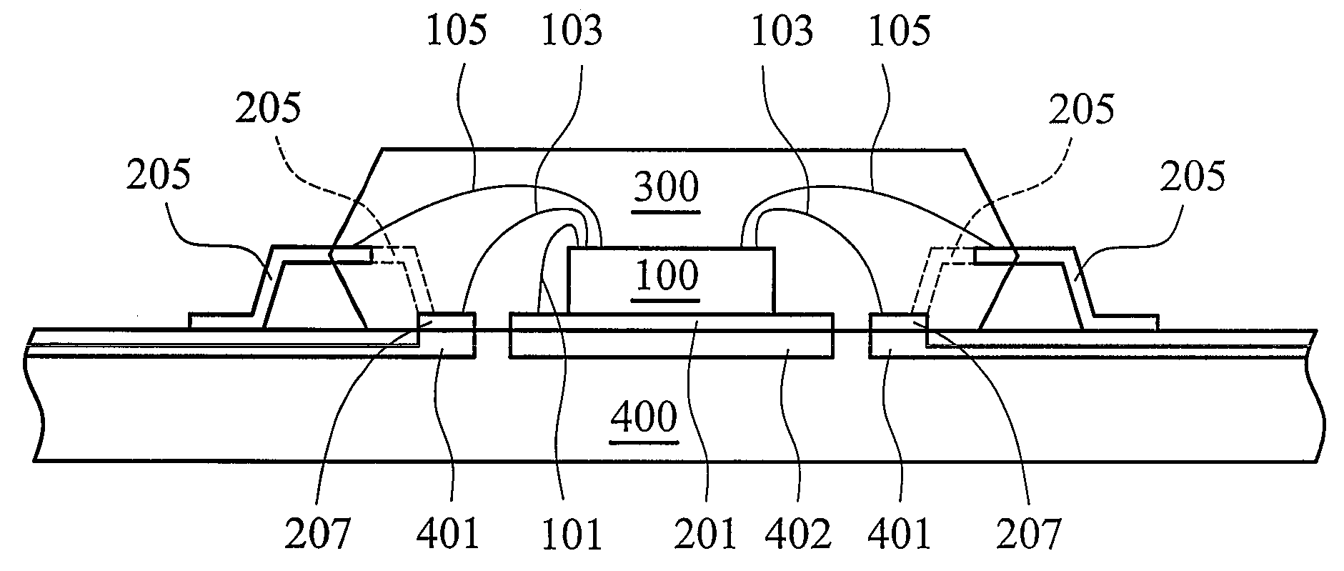
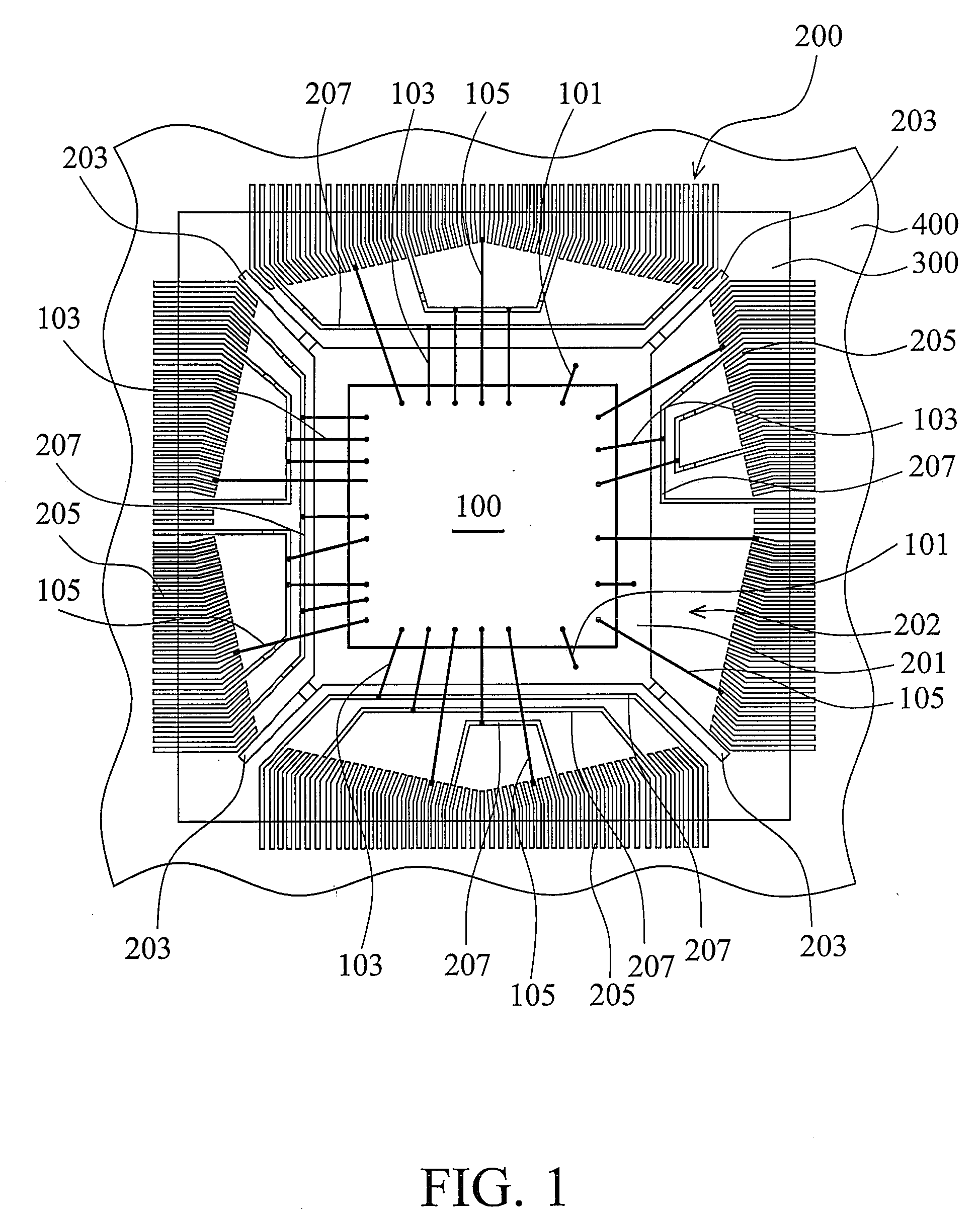
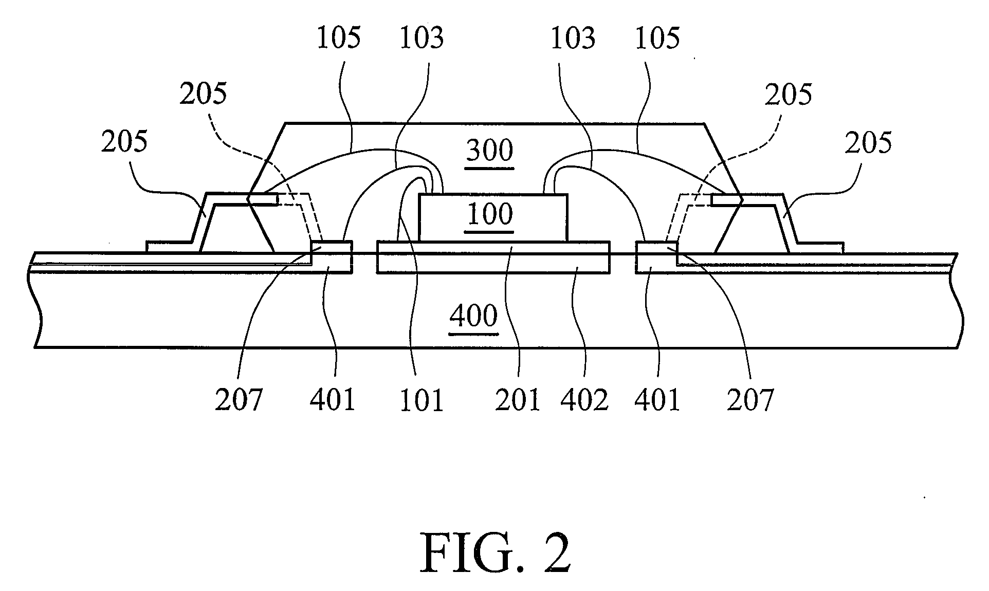
[0016]Referring to FIGS. 1 and 2, in which FIG. 1 illustrates a plan view of an embodiment of an electronic device with a package body according to the invention and FIG. 2 illustrates a cross section of the electronic device shown in FIG. 1. The electronic device comprises an electronic package boned on a circuit board 400, such as a package substrate or a print circuit board (PCB). In this embodiment, the electronic package is an exposed-pad quad flat package (QFP).

[0017]In the embodiment, the electronic package comprises a die 100 including integrated circuits, a leadframe 20...


PUM


Abstract

An electronic package is provided. The electronic package comprises a die pad having a die attached thereon. A plurality of leads surrounds the die pad and spaced therefrom to define a ring gap therebetween. At least one first common electrode bar is in the ring gap and substantially coplanar to the die pad, in which at least one of the plurality of leads extends to the first common electrode bar. A molding compound partially encapsulates the die pad and the first common electrode bar, such that the bottom surfaces of the die pad and the first common electrode bar are exposed. An electronic device with the electronic package is also disclosed.

Description

CROSS REFERENCE TO RELATED APPILCATIONS[0001]This application claims the benefit of U.S. Provisional Application No. 60 / 950,363, filed Jul. 18, 2007, the entirety of which is incorporated by reference herein.BACKGROUND OF THE INVENTION[0002]1. Field of the Invention[0003]The invention relates to electronics packaging technology and in particular to an exposed-pad quad flat package (QFP) having exposed common electrode bars and an electronic device including the package.[0004]2. Description of the Related Art[0005]Driven by miniaturization of highly integrated and advanced semiconductor devices, requirement for higher density packaging has increased. For this purpose, semiconductor manufacturers must provide semiconductor packages having thinner profiles. In the highly integrated and advanced semiconductor devices, to process signals at a high speeds, the heat developed in the dies and the inductance in package cannot be ignored. Thus, heat dissipation and lowering inductance are two...

Claims


Application Information

Patent Timeline
Patent Type & Authority Applications(United States)
IPC IPC(8): H01L23/495
CPCH01L23/3107H01L2224/49109H01L23/49551H01L24/49H01L2224/48091H01L2224/48247H01L2224/48257H01L2224/4911H01L2924/01002H01L2924/01013H01L2924/01015H01L2924/01029H01L2924/01033H01L2924/01077H01L2924/01082H01L2924/14H01L2924/19107H01L2924/30107H01L23/49541H01L2924/01006H01L24/48H01L2924/00014H01L2924/181H01L2224/45099H01L2224/05599H01L2924/00012
Inventor CHEN, NAN-CHENGCHEN, NAN-JANGLI, CHING-CHIH
Owner MEDIATEK INC
Why Eureka
Try Eureka