Wafer level stacked packages with individual chip selection
a technology of stacked packages and chips, applied in the direction of electrical equipment, semiconductor devices, semiconductor/solid-state device details, etc., can solve the problems of affecting the quality of stacked packages, the disadvantage of complexity, cost, thickness and testability of stacked packages
- Summary
- Abstract
- Description
- Claims
- Application Information
AI Technical Summary
Problems solved by technology
Method used
Image
Examples
Embodiment Construction
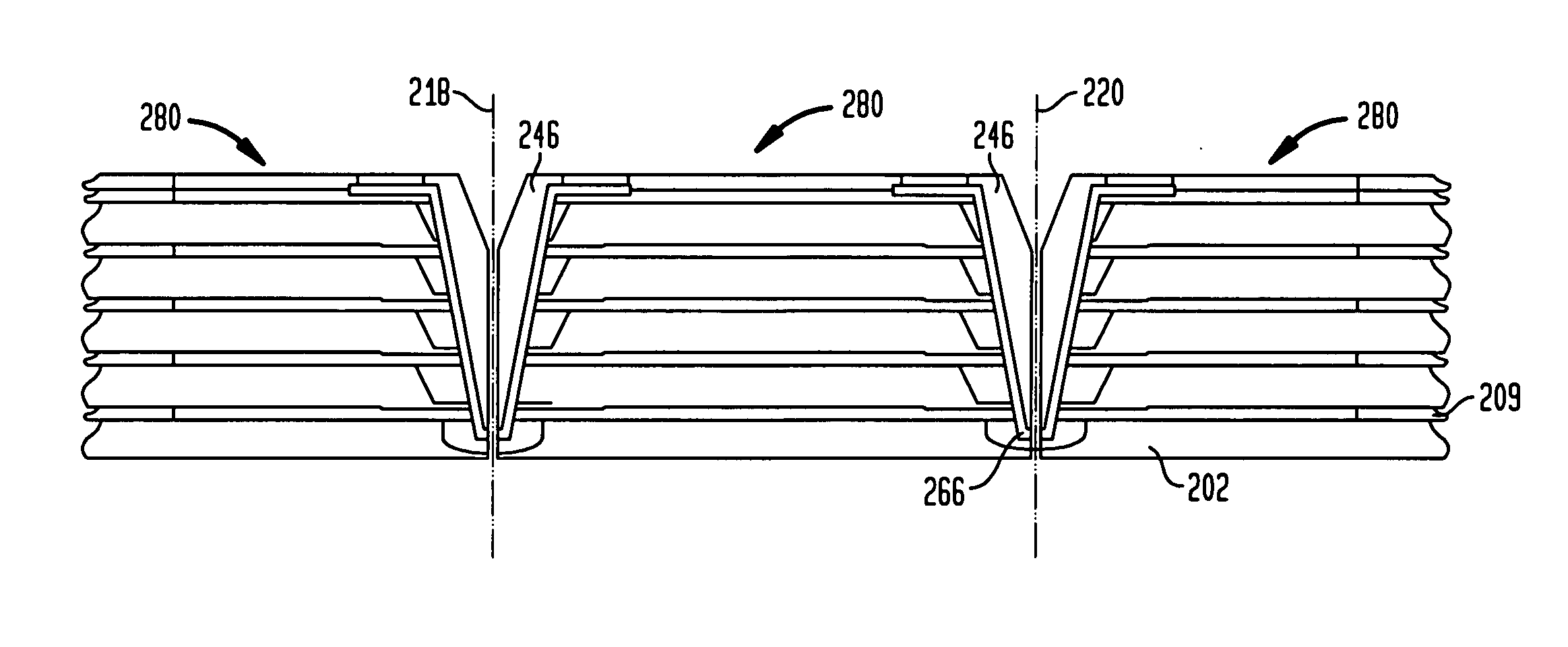
[0043]Accordingly, embodiments of the invention herein provide ways of forming stacked assemblies containing a plurality of stacked microelectronic elements. In one embodiment, leads extend along edges of each resulting stacked assembly, where the leads from one microelectronic element extending along one edge of the assembly are laterally spaced from the leads of other microelectronic elements which extend along that edge. In this way, electrical isolation can be provided between the leads of each microelectronic element at that edge.
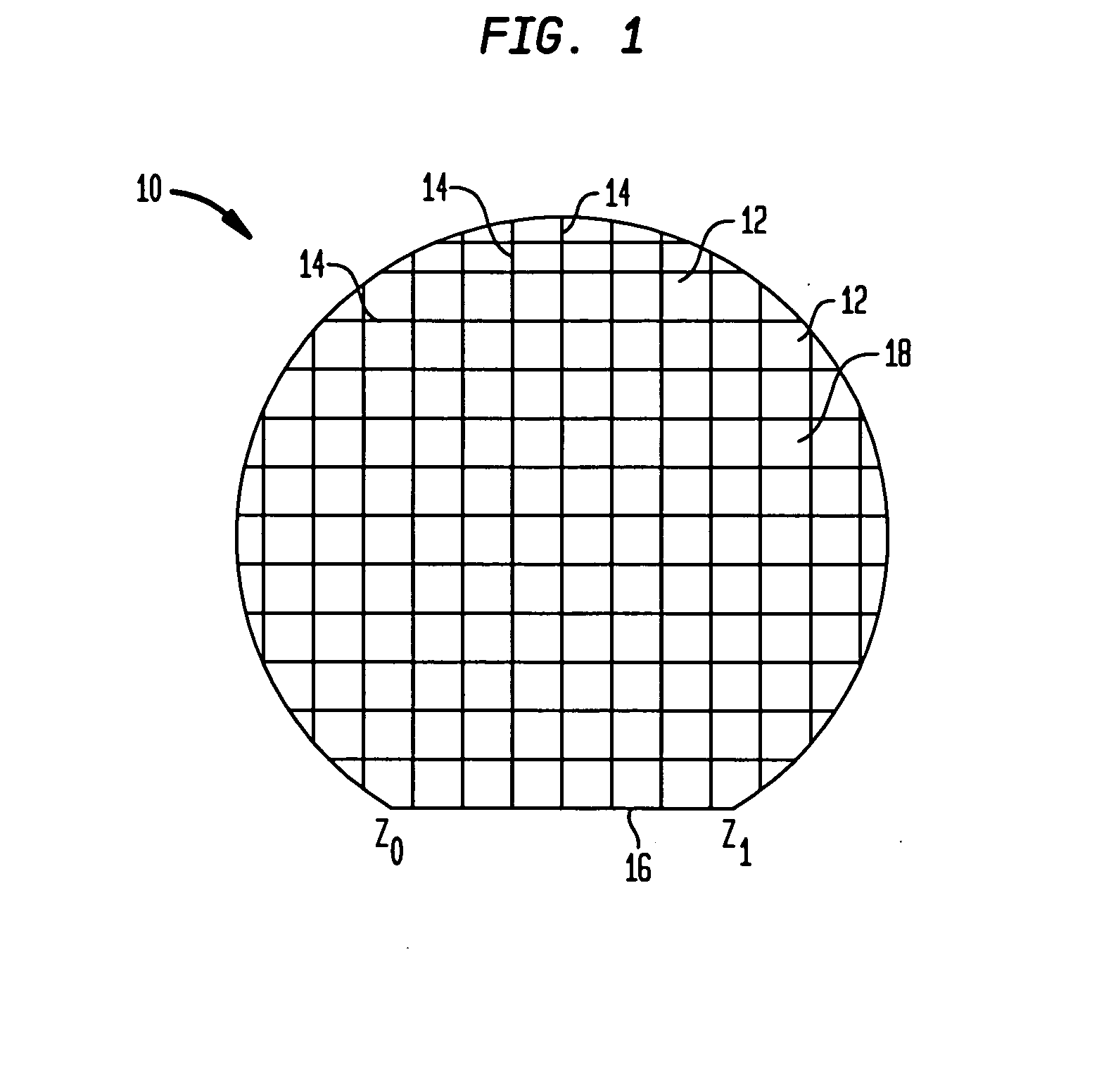
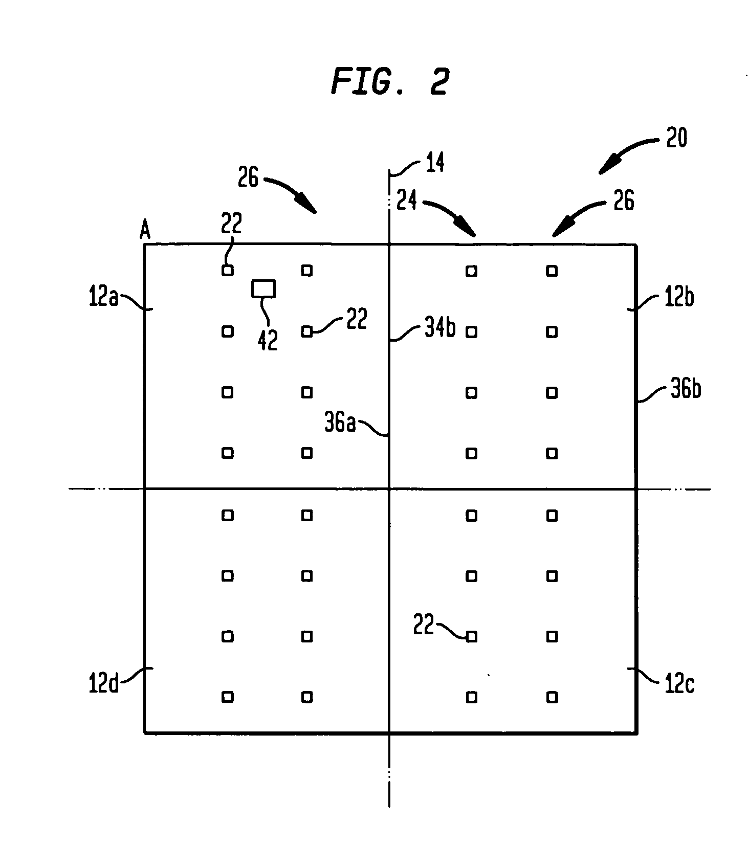
[0044]A wafer-level method will now be described for fabricating a plurality of stacked assemblies. FIG. 1 is a top plan view illustrating a microelectronic substrate such as a semiconductor device wafer 10. The wafer 10 includes a plurality of microelectronic elements 12, e.g., semiconductor device chips, passive device chips, or combination chips including both active and passive devices, etc., which are attached together at dicing lanes 14. The micr...
PUM
 Abstract
Description
Claims
Application Information


