

Electric current driving type display device
- Summary
- Abstract
- Description
- Claims
- Application Information
AI Technical Summary
Benefits of technology
Problems solved by technology
Method used
Image

Examples
first embodiment
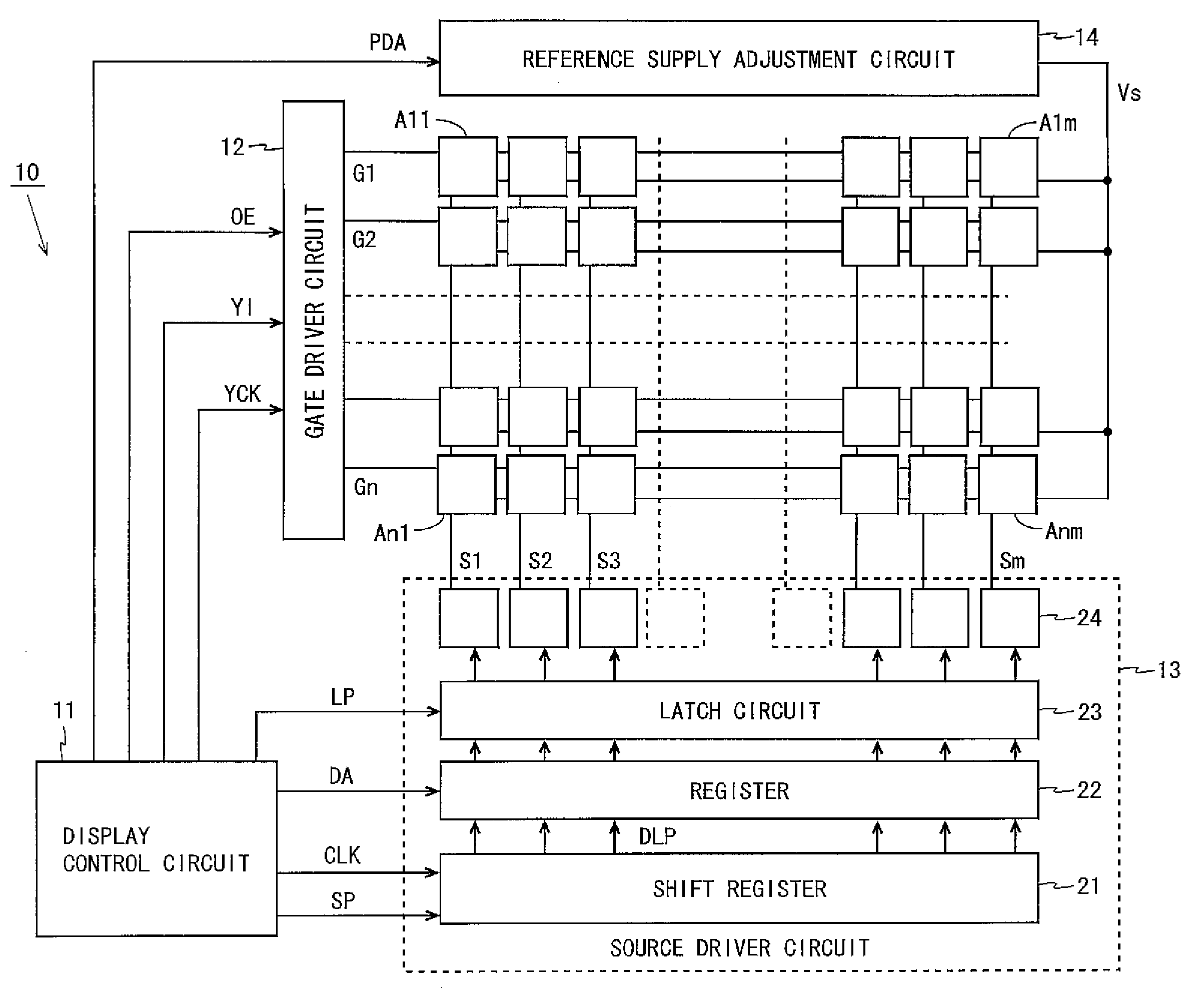
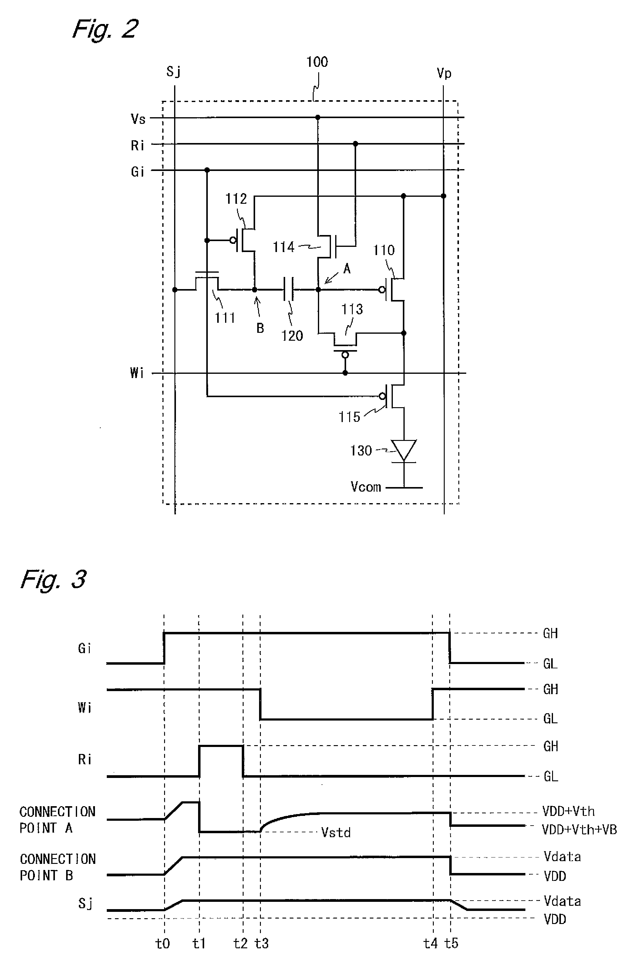
[0135]FIG. 2 is a circuit diagram of a pixel circuit included in a display device according to the first embodiment of the present invention, A pixel circuit 100 shown in FIG. 2 includes a driving TFT 110, switching TFTs 111 to 115, a capacitor 120, and an organic EL element 130. The switching TFTs 111 and 114 are of an n-channel type and other TFTs are of a p-channel type.
[0136]The pixel circuit 100 is connected to a power supply wiring line Vp, a reference supply wiring line Vs, a common cathode Vcom, a scanning line Gi, control lines Wi and Ri, and a data line Sj. Of them, to the power supply wiring line Vp (first power supply wiring line) and the common cathode Vcom (second power supply wiring line) are respectively applied fixed potentials VDD and VSS and to the reference supply wiring line Vs (third power supply wiring line) is applied a reference potential Vstd obtained by the reference supply adjustment circuit 14. The common cathode Vcom serves as a common electrode for all...
second embodiment
[0158]FIG. 4 is a circuit diagram of a pixel circuit included in a display device according to the second embodiment of the present invention. A pixel circuit 200 shown in FIG. 4 includes a driving TFT 210, switching TFTs 211 to 214, a capacitor 220, and an organic EL element 230. The switching TFTs 211 and 214 are of an n-channel type and other TFTs are of a p-channel type.
[0159]The pixel circuit 200 is obtained by making a change to the pixel circuit 100 (FIG. 2) according to the first embodiment such that the switching TFT 115 is eliminated and a cathode terminal of the organic EL element 130 is connected to a cathode wiring line CAi (second power supply wiring line). In the pixel circuit 200, on a path connecting a power supply wiring line Vp to the cathode wiring line CAi, in order from the side of the power supply wiring line Vp, the driving TFT 210 and the organic EL element 230 are provided in series. Except for the above points, the configuration of the pixel circuit 200 is...
third embodiment
[0163]FIG. 6 is a circuit diagram of a pixel circuit included in a display device according to the third embodiment of the present invention. A pixel circuit 300 shown in FIG. 6 includes a driving TFT 310, switching TFTs 311 to 315, a capacitor 320, and an organic EL element 330. All of the TFTs included in the pixel circuit 300 are of a p-channel type.
[0164]The pixel circuit 300 is obtained by making a change to the pixel circuit 100 (FIG. 2) according to the first embodiment such that the TFTs of an n-channel type are changed to TFT of a p-channel type and a gate terminal of each TFT is connected to an appropriate signal line. In the pixel circuit 300, gate terminals of the respective switching TFTs 311 and 313 are connected to a scanning line Gi, gate terminals of the respective switching TFTs 312 and 315 are connected to a control line Ei, and a gate terminal of the switching TFT 314 is connected to a control line Ri. Except for the above points, the configuration of the pixel c...
PUM
 Abstract
Description
Claims
Application Information