Method for manufacturing liquid discharge head substrate
- Summary
- Abstract
- Description
- Claims
- Application Information
AI Technical Summary
Benefits of technology
Problems solved by technology
Method used
Image
Examples
first embodiment
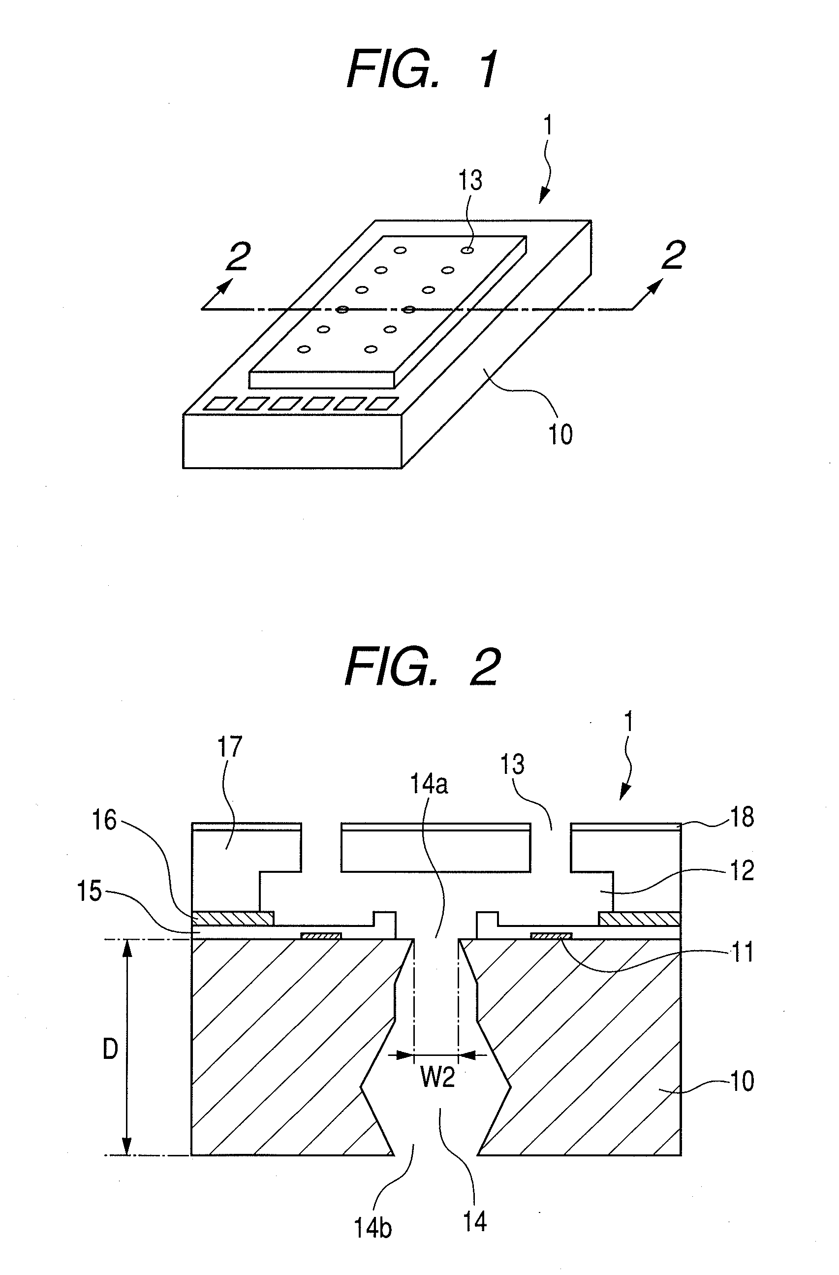
[0029]For the sake of convenience, a descriptive overview will be given for a liquid discharge head substrate produced using a liquid discharge head substrate manufacturing method of a first embodiment of this invention, and the structure of a liquid discharge head for which this substrate is employed. FIG. 1 is a schematic perspective view of an inkjet head substrate 1, an example liquid discharge head produced using the manufacturing method of the first embodiment. And FIG. 2 is a cross-sectional view of the inkjet head substrate 1 taken along line 2-2 in FIG. 1.
[0030]The inkjet head substrate 1 (hereinafter referred to also as a head substrate) includes a silicon substrate 10, on the obverse side of which are formed multiple energy generation elements 11, such as heaters, and ink flow passageways 12 and discharge ports 13. Further, an ink supply port 14 passes through the silicon substrate 10, opening out on both the obverse and reverse sides.
[0031]More specifically, the energy g...
second embodiment
[0057]A head substrate manufacturing method according to a second embodiment of the present invention will now be described while referring to FIGS. 5 and 6. FIG. 5 is a schematic cross-sectional view of the processing performed for the manufacturing method of the second embodiment. And FIG. 6 is a schematic cross-sectional view of a head substrate obtained by employing the manufacturing method of this embodiment.
[0058]The head substrate manufacturing method of this embodiment basically provides the same processing as the manufacturing method of the first embodiment. The only difference is the length of a period required for orientation-dependent anisotropic etching to form a recessed portion (a non-perforating hole) 26 that later becomes an ink supply port 14. Specifically, as illustrated in FIG. 5, orientation-dependent anisotropic etching is performed for a shorter period than in the first embodiment, and a second recessed portion 26 is formed. As a result, as illustrated in FIG....
third embodiment
[0059]A head substrate manufacturing method according to a third embodiment of the present invention will now be described while referring to FIGS. 7 and 8. FIG. 7 is a schematic cross-sectional view of the processing performed by the manufacturing method of the third embodiment, and FIG. 8 is a schematic cross-sectional view of a head substrate obtained using the manufacturing method of the embodiment.
[0060]The head substrate manufacturing method of this embodiment provides the same processing as that of the first embodiment. The only difference is that the anisotropic etching process is performed in three steps to form a recessed portion (a non-perforating hole) 26 that will later be an ink supply port 14.
[0061]Specifically, according to the manufacturing method of the first embodiment, orientation-dependent anisotropic wet etching and anisotropic dry etching have been performed for the silicon substrate 10, in the named order, to form the second recessed portion 26. However, acco...
PUM
| Property | Measurement | Unit |
|---|---|---|
| Thickness | aaaaa | aaaaa |
Abstract
Description
Claims
Application Information


