Optical encoder and electronic equipment having the same

a technology of optical encoder and electronic equipment, applied in the direction of discharge tube/lamp details, instruments, material analysis, etc., can solve the problems of varying the duty ratio of output signals, affecting the accuracy of output signals, and inevitably occurring a 1-gate delay in logic circuits

Active Publication Date: 2009-03-19
SHARP KK
View PDF17 Cites 3 Cited by
  • Summary
  • Abstract
  • Description
  • Claims
  • Application Information

AI Technical Summary

Benefits of technology

[0013]Accordingly, an object of the present invention is to provide an optical encoder which is enabled to avoid occurrence of phase differences among signals due to gate delay and to detect the mover with signals of excellent duty precision and periodic precision.

Problems solved by technology

However, in the case where two pulse signals are EXCLUSIVE-ORed as shown above, there inevitably occurs a 1-gate delay within the logic circuit.
In ordinary logic circuits, that delay falls within an error range.
However, in a light receiving circuit including light receiving elements that treat weak signals, the 1-gate delay causes impedance differences between signal input and output, which leads to variations in the duty ratio of an output signal, with the periodic fluctuation increased.
As a result, there is a problem that merits by twice higher resolutions could not be obtained.
Also, in JP H3-37518 A, logically combining a signal obtained by EXCLUSIVE-ORing with an original signal before the logical operation of EXCLUSIVE-ORing would involve a further gate delay, resulting in a easier occurrence of malfunction.

Method used


Image

  • Optical encoder and electronic equipment having the same
  • Optical encoder and electronic equipment having the same
  • Optical encoder and electronic equipment having the same

Examples


first embodiment

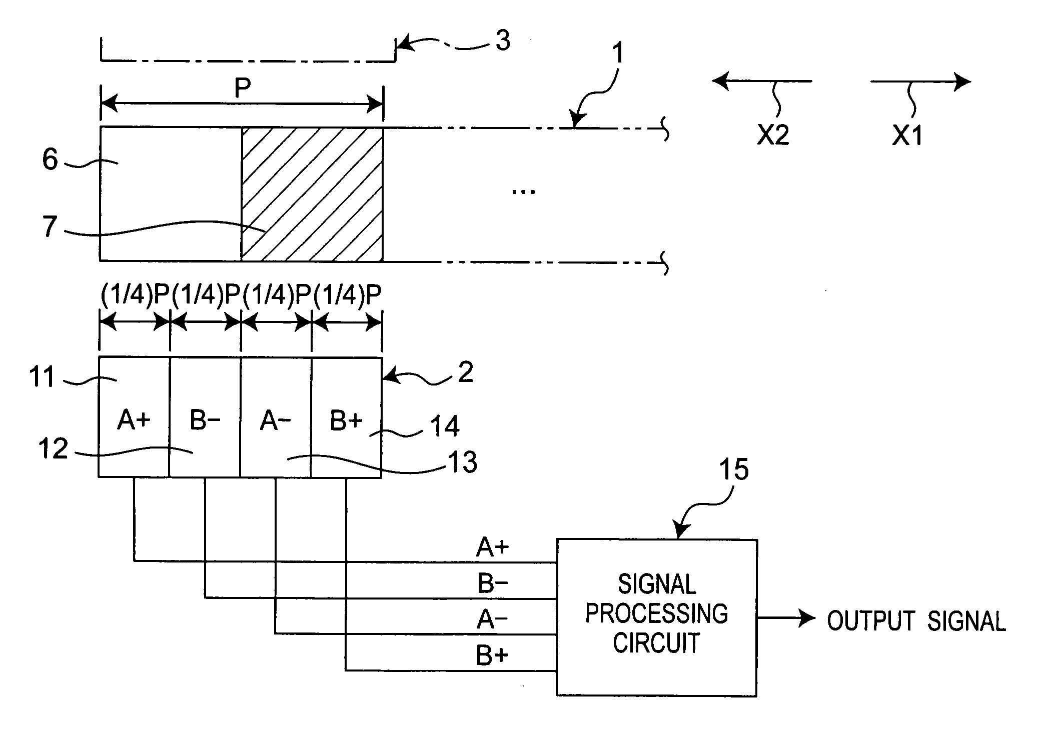
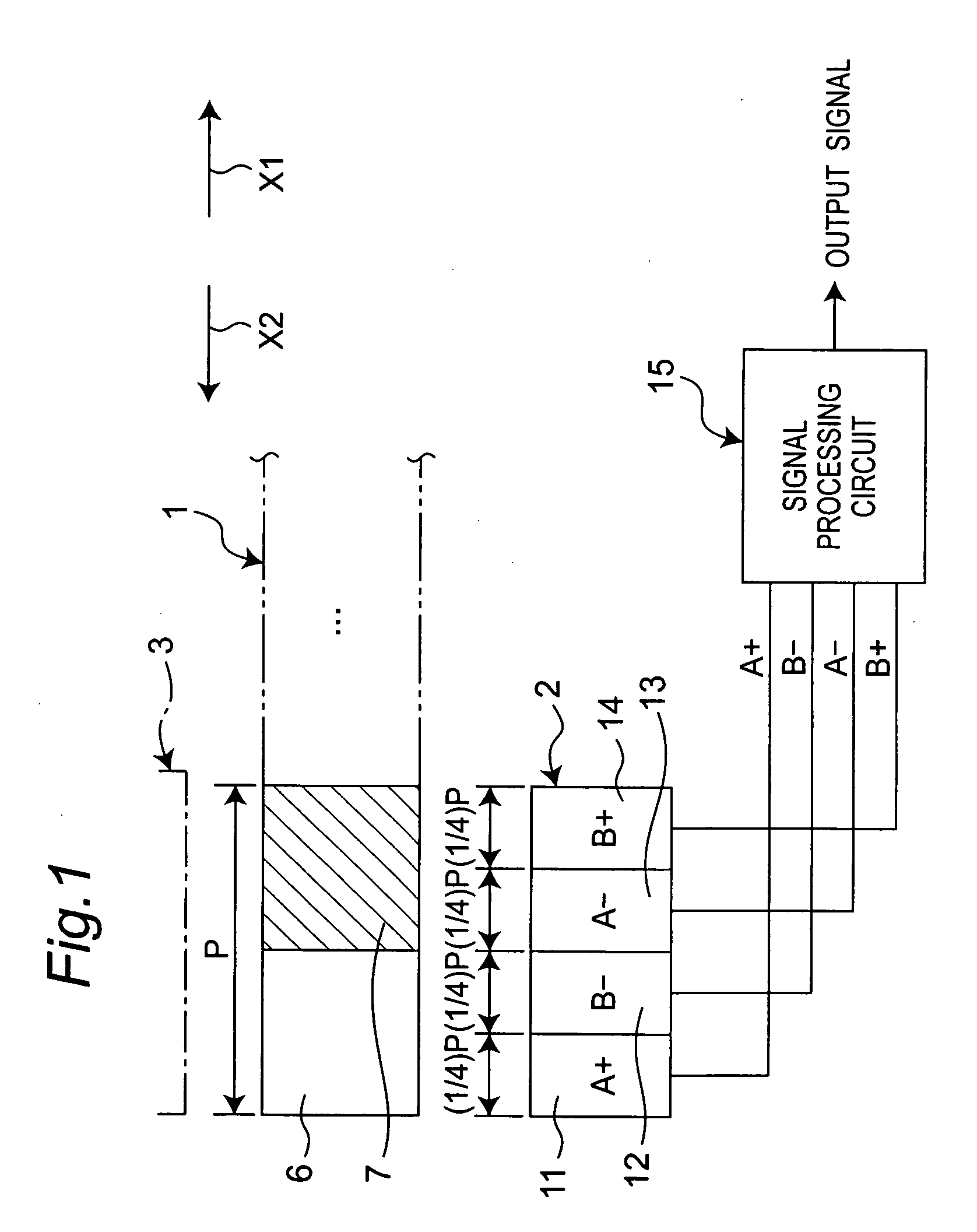
[0059]FIG. 1 shows an outlined configuration of a first embodiment of the optical encoder of the invention. The first embodiment includes a mover 1, a light receiving section 2 and a light emitting section 3. The light emitting section 3 is composed of light emitting elements such as LEDs (light emitting diodes).

[0060]The light receiving section 2 has four light receiving elements 11-14. For higher resolutions, the light receiving section 2 may also include a larger number, such as 8 or 16, of light receiving elements arranged therein. The mover 1 is movable in a direction indicated by arrow X1 or X2, where light-on portions 6 and light-off portions 7 are alternately arrayed along the moving direction. Given an array pitch P of the light-on portions 6, each of the light-on portions 6 and the light-off portions 7 has a size in the moving direction (width) equal to (½)P. The light-on portions 6 transmit light derived from the light emitting section 3 toward the light receiving section...

second embodiment

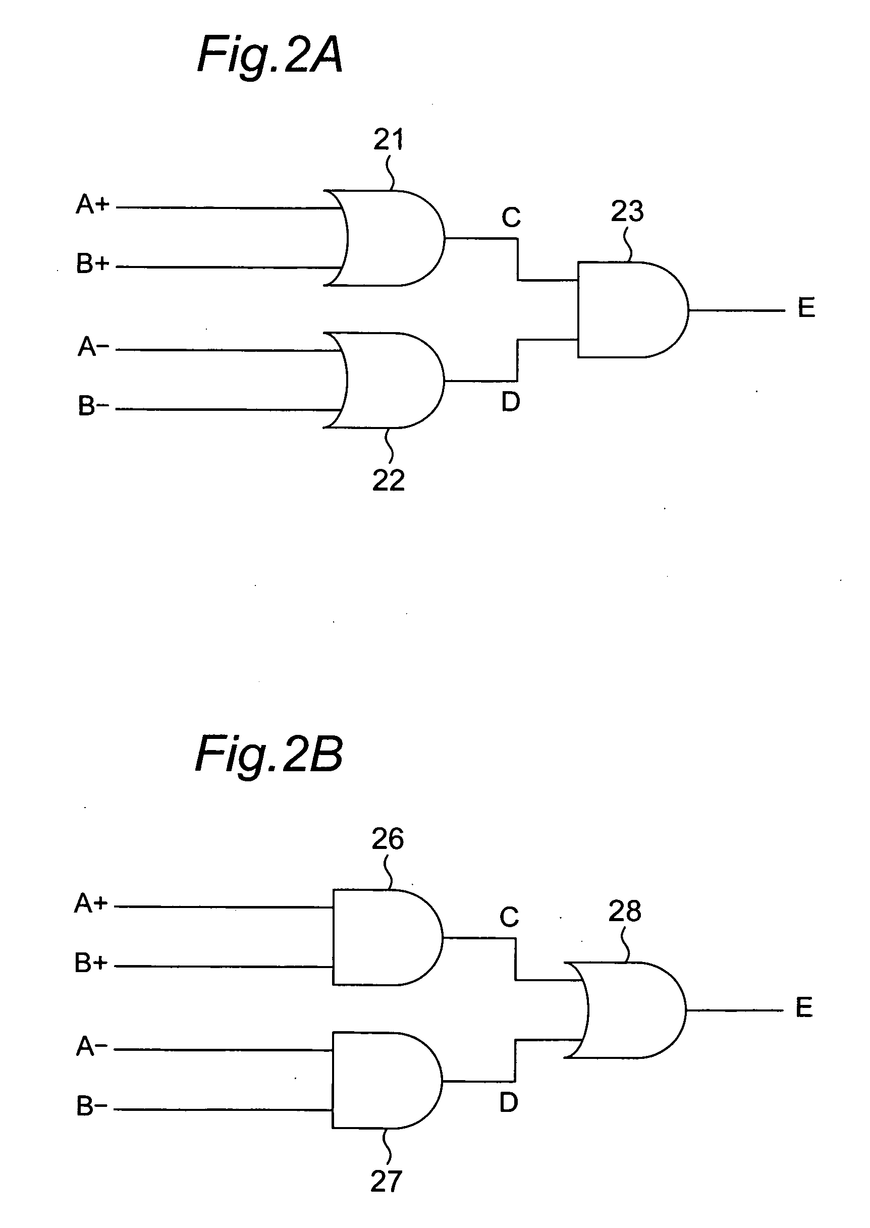
[0068]Next, FIG. 2B shows a structure of a signal processing circuit included in a second embodiment of the optical encoder of the invention. This second embodiment differs from the foregoing first embodiment only in that a signal processing circuit shown in FIG. 2B is provided instead of the signal processing circuit shown in FIG. 2A of the first embodiment. Therefore, differences from the first embodiment will mostly be described in this second embodiment.

[0069]The signal processing circuit included in the second embodiment, as shown in FIG. 2B, has a first AND circuit 26, a second AND circuit 27, and an OR circuit 28. Inputted to the first AND circuit 26 are light reception signals A+ and B++which are different in phase by 90° from each other. Also, inputted to the second AND circuit 27 are light reception signals A− and B− which are different in phase by 90° from each other.

[0070]Therefore, the first AND circuit 26 computes a logical AND of the light reception signal A+ and the ...

third embodiment

[0093]Next, FIG. 7 shows a structure of a signal processing circuit included in a third embodiment of the optical encoder of the invention. This third embodiment differs from the foregoing first embodiment only in that a signal processing circuit shown in FIG. 7 is provided instead of the signal processing circuit shown in FIG. 2A of the first embodiment. Therefore, differences from the first embodiment will mostly be described in this third embodiment.

[0094]The signal processing circuit included in this third embodiment, as shown in FIG. 7, has first to fourth inverters 81-84, a fifth inverter 85 to which outputs of the first, second inverters 81, 82 are inputted, and a sixth inverter 86 to which outputs of the third, fourth inverters 83, 84 are inputted. The signal processing circuit also has a seventh inverter 87 to which outputs of the fifth, sixth inverters 85, 86 are inputted, and an eighth inverter 88 to which an output of the seventh inverter 87 is inputted.

[0095]The signal ...


PUM


Abstract

An optical encoder of the invention has an OR circuit 21 to which light reception signals A+, B+ are inputted, an OR circuit 22 to which light reception signals A−, B− are inputted, and an AND circuit 23 to which an output signal C of the OR circuit 21 and an output signal D of the OR circuit 22 are inputted. In this optical encoder, a light reception signal A− shifted in phase by 180° from the light reception signal A+, and a light reception signal B− shifted in phase by 180° from the light reception signal B+, are inputted to the OR circuit 22 of the signal processing circuit 15. Thus, the signal processing circuit 15 does not need NOT circuits for inverting the light reception signal A+ and B+. This optical encoder can avoid occurrence of phase differences due to gate delay among signals and detect the mover with signals of excellent duty and periodic precisions.

Description

CROSS-REFERENCE TO RELATED APPLICATIONS[0001]This nonprovisional application claims priority under 35 U.S.C. §119(a) on Patent Application No(s). 2007-231227 filed in Japan on Sep. 6, 2007, the entire contents of which are hereby incorporated by reference.BACKGROUND OF THE INVENTION[0002]The present invention relates to an optical encoder for detecting position, moving speed, moving direction and the like of a mover with use of light receiving elements. In particular, the invention relates to an optical encoder suitable for use in copiers, printers or other printing devices, FA (Factory Automation) equipment, and the like.[0003]Conventionally, JP H1-136019 A discloses an encoder in which pulse signals having a phase difference of 90° are inputted to an EXCLUSIVE-OR circuit, allowing a resolution twice higher than conventional ones to be obtained.[0004]Also, JP H1-156621 A discloses an optical encoder in which four signals different in phase by 45° are inputted to an EXCLUSIVE-OR cir...

Claims


Application Information

Patent Timeline
Patent Type & Authority Applications(United States)
IPC IPC(8): G01D5/34
CPCG01D5/36
Inventor OKADA, NORIKAZU
Owner SHARP KK
Why Eureka
Try Eureka