A Broadband Radio Frequency Signal Generation System
A radio frequency signal and generation system technology, applied in the field of communication, can solve the problems of not being able to directly generate radio frequency signals, not being able to generate radio frequency signals, and the flexibility of generating signals is not high, and achieve simple and flexible implementation methods, overcome clock rate mismatch, Bandwidth effect
- Summary
- Abstract
- Description
- Claims
- Application Information
AI Technical Summary
Problems solved by technology
Method used
Image
Examples
Embodiment 1
[0037] This embodiment provides a broadband radio frequency signal generation system, such as figure 1 , including the host computer, PCIe bus, FPGA main board, and DAC board. The host computer is used to generate digital signals and transmit the digital signals to the FPGA main board through the PCIe bus. The FPGA main board transmits the digital signals to the DAC board through the control logic unit;
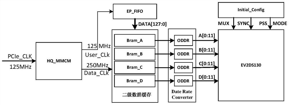
[0038] Such as image 3 , the control logic unit includes: a clock management module, a data cache module, a secondary data cache module, a data rate conversion module, and an initialization configuration logic module;
[0039] The clock management module is used to receive the 125MHz clock signal from the PCIe bus, divide and process the 125MHz clock signal into one 125MHz clock signal and one 250MHz clock signal, transmit one 125MHz clock signal to the data cache module, and transfer one A 250MHz clock signal is transmitted to the secondary data cache module;
[0040]Desi...
Embodiment 2
[0048] The present embodiment provides the concrete structure of upper computer on the basis of embodiment 1, comprises board card control module, parameter input and data generation module, waveform chart drawing module; Described board card control module is used to provide to user interface to control The status of the DAC board card and the RF signal sampling data generated by the user are sent to the signal board to correctly generate the signal. The parameter input and data generation module is used for this module to provide the user with a visual interface to select the interference signal style that needs to be generated and Corresponding parameters, and call MATLAB according to the input parameters to complete the generation of signal sampling data files; the waveform diagram drawing module is used to draw the time domain waveform diagram and spectrum diagram of the interference signal designed by the user, so that the user can observe designed interference signal.
...
Embodiment 3
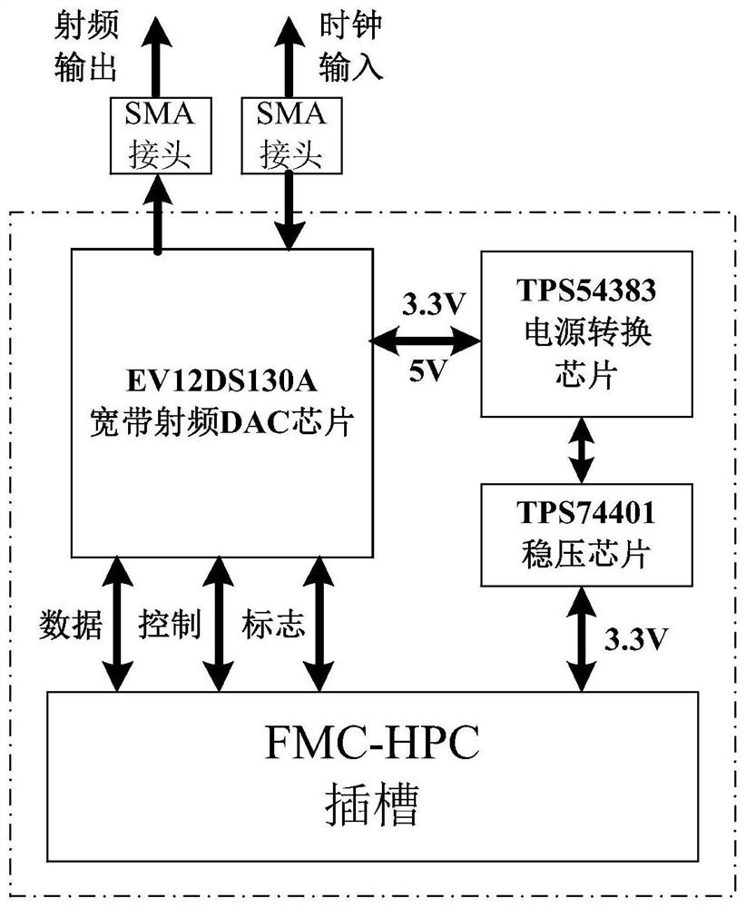
[0061] This embodiment provides the specific structure of the DAC board on the basis of Embodiment 1, such as figure 2 , DAC board includes DAC chip, power conversion chip, voltage regulator chip and FMC-HPC interface, FMC-HPC interface is used to convert 3.3V power supply to 5V voltage, 5V voltage passes through voltage regulator chip, power conversion chip and DAC chip electrical connection;
[0062] The external clock signal is input into the DAC chip through the SMA connector, and the DAC video signal is output through the SMA connector.
[0063] The DAC board is based on the EV12DS130A chip, which can directly have an analog output bandwidth of 7GHz without relying on the up-converter module. It also has 12-bit resolution and four different operating modes of RTZ, NRZ, NRTZ, and RF to choose from. Its clock resolution Reaching 0.0625Hz, the operation of the board is simple and flexible, and there are reserved configuration and status observation bit ports. In order to ...
PUM
 Abstract
Description
Claims
Application Information


