Apparatus and method for picking-up semiconductor dies

a technology of semiconductor dies and pickup devices, which is applied in the direction of semiconductor/solid-state device manufacturing, electric devices, basic electric elements, etc., can solve the problems of force breaking or deformation of semiconductor dies, the method of using push-up needles is less suitable for picking up thin semiconductor dies, and the force is not strong enough to break or deform semiconductor dies. , to achieve the effect of easy picking up a semiconductor di

Inactive Publication Date: 2009-03-19
SHINKAWA CO LTD
View PDF2 Cites 36 Cited by
  • Summary
  • Abstract
  • Description
  • Claims
  • Application Information

AI Technical Summary

Benefits of technology

[0009]In view of the above problems, an object of the present invention is to provide a die pick-up apparatus and method for picking up a semiconductor die easily while controlling a force exerted to the semiconductor die during peeling off of a dicing sheet.

Problems solved by technology

However, this method that uses a push-up needle has become less suitable for picking up thin semiconductor dies of recent years, because the method poses a problem that the pushing up can break the semiconductor dies as the dies become thinner.
However, once peeled off from the semiconductor die, the dicing tape covers the suction hole, and consequently it is not possible to suction the air around the suction hole after peeling a portion of the dicing tape immediately above the suction hole.
Suctioning the dicing sheet through such a large suction hole may, when adhesive force of the dicing sheet is large, produce a large force that is exerted to the semiconductor die, and such a large force may break or deform the semiconductor die, especially because semiconductor dies of recent years are made thin with less intensity.
As described above, with the method disclosed in Japanese Patent No. 3209736, it is unable to control the force exerted to the semiconductor die during the peeling off of the dicing sheet, because a large force is applied to the semiconductor die during the suctioning when a large suction hole is used, and during the movement of the die stage when a small suction hole is used, and thus the method poses a problem that the semiconductor die can be damaged.
In addition, there is a case in which the semiconductor die cannot be picked up smoothly because the dicing sheet remains unpeeled on the end surface of the semiconductor die facing toward the direction in which the protrusion moves.
However, there is a problem that the protrusion can be brought into contact with an adjacent semiconductor die to damage the semiconductor die when the adjacent semiconductor die is present in the direction in which the protrusion moves, and thus the direction in which the protrusion moves is limited.

Method used


Image

  • Apparatus and method for picking-up semiconductor dies
  • Apparatus and method for picking-up semiconductor dies
  • Apparatus and method for picking-up semiconductor dies

Examples


Embodiment Construction

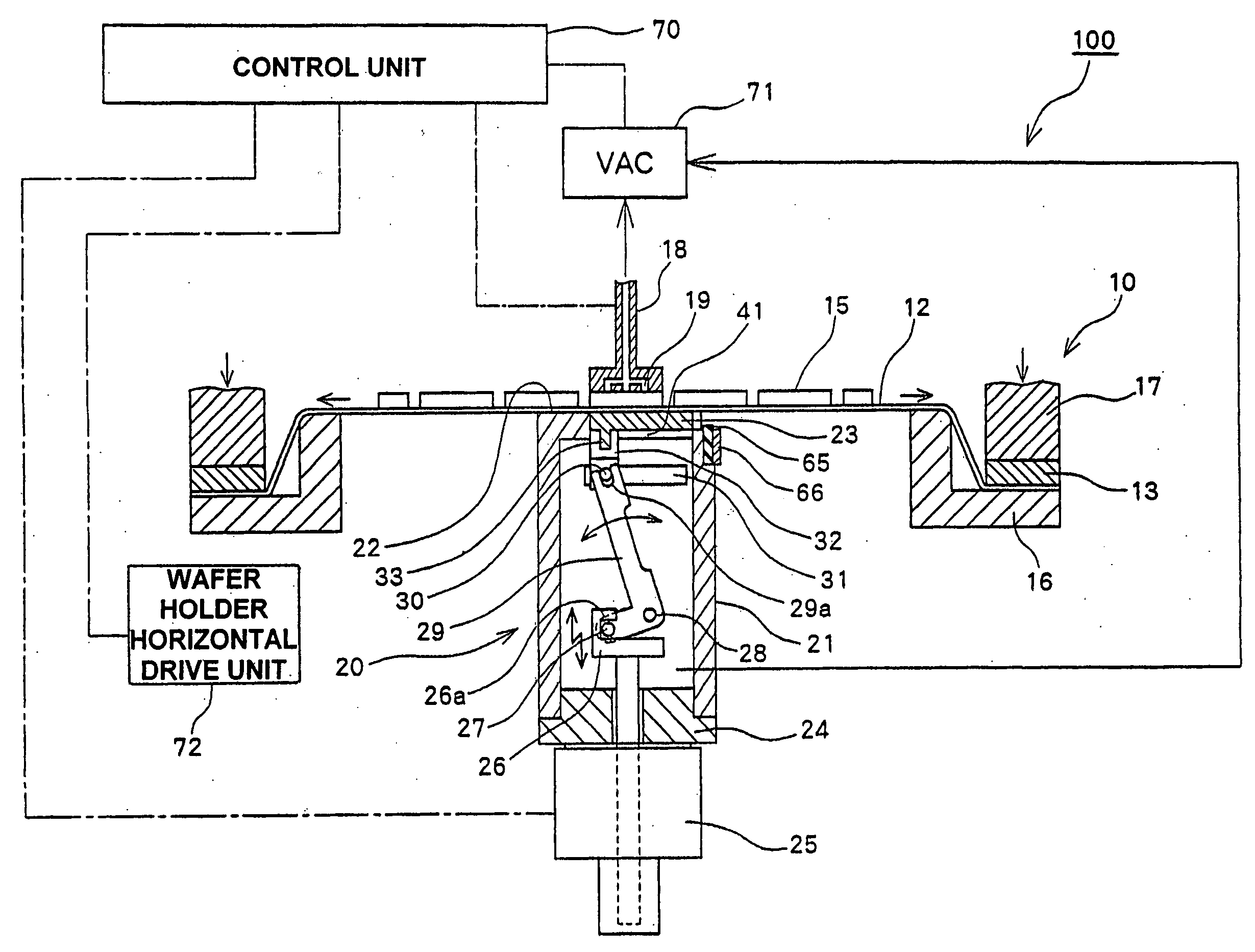
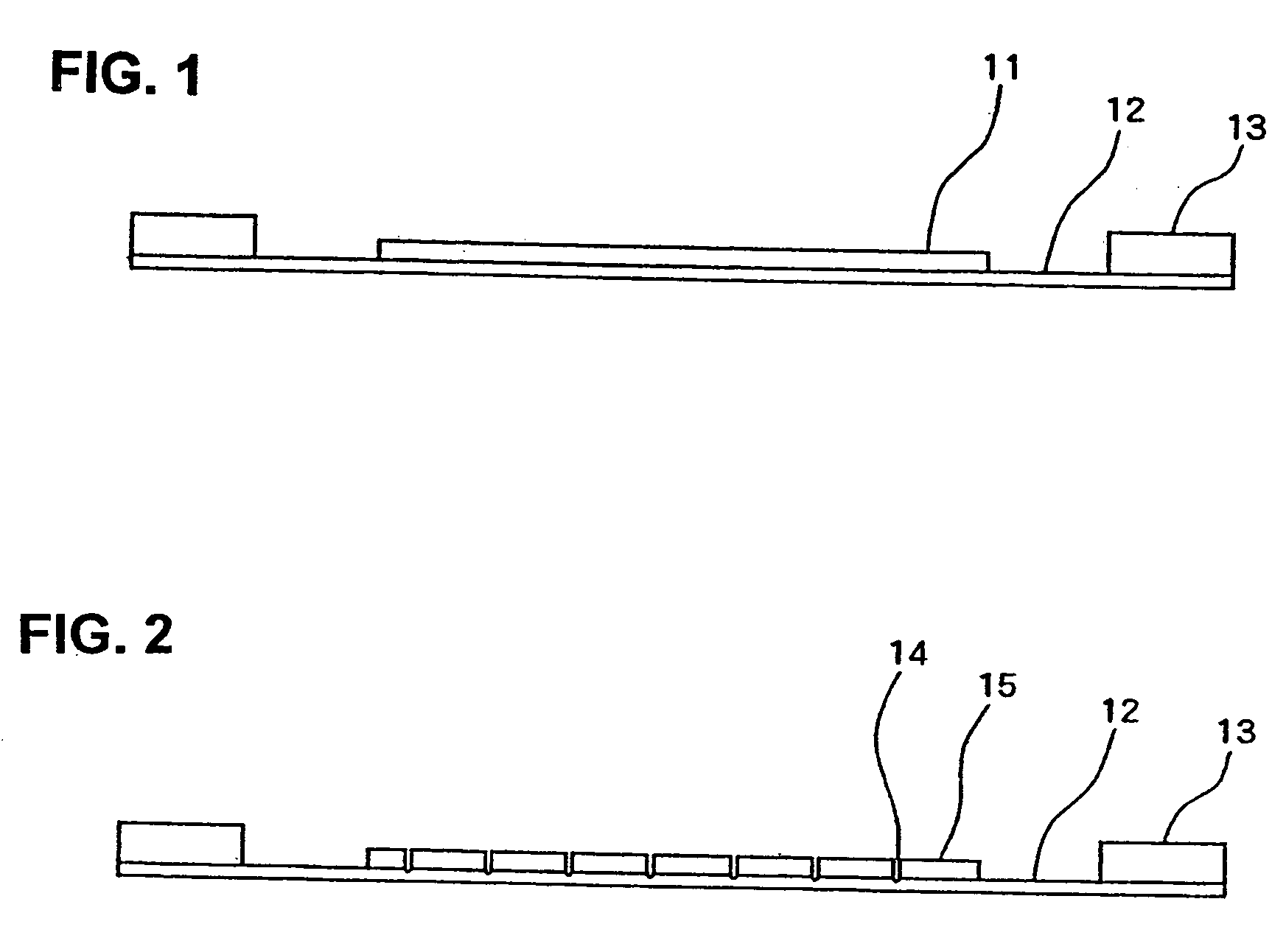
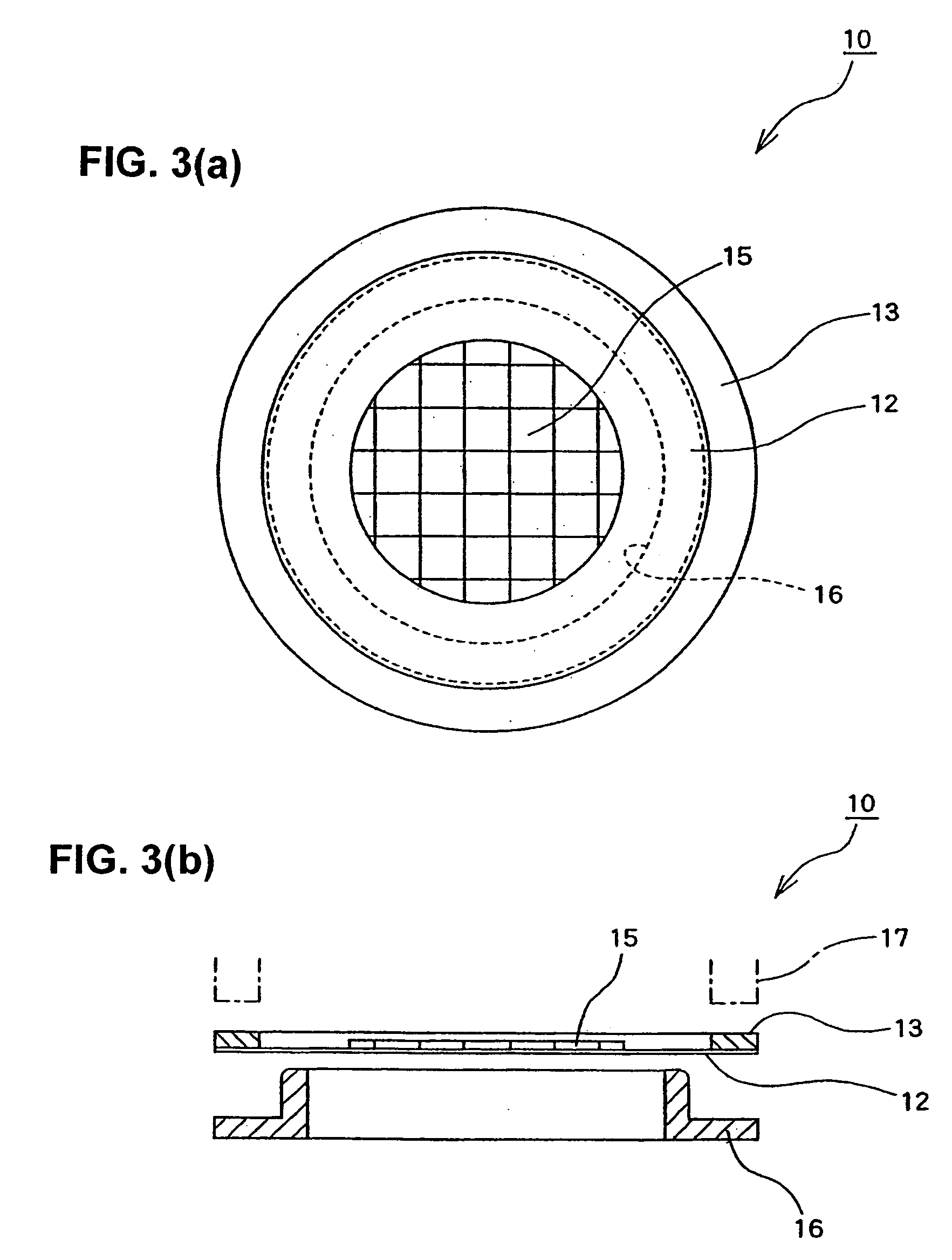
[0082]The preferred embodiments of the present invention will be described in detail below with reference to the accompanying drawings. Before describing a die pick-up apparatus for picking up semiconductor dies according to the present invention, an explanation will be given first on a wafer and a wafer holder.

[0083]Referring to FIG. 1, a wafer 11 is applied with an adhesive dicing sheet 12 on a back side thereof, and the dicing sheet 12 is attached to a metal ring 13. The wafer 11 is handled while being attached to the metal ring 13 with the dicing sheet 12 therebetween as shown in the drawings. Then, as shown in FIG. 2, the wafer 11 is diced, in a dicing step, into semiconductor dies 15 from the other side using, for example, a dicing saw. Between each pair of the semiconductor dies 15 is a cutting gap 14 that is formed during the dicing, and while the cutting gap 14 reaches a part of the dicing sheet 12 through the semiconductor dies 15, the dicing sheet 12 is not totally cut ap...


PUM

PropertyMeasurementUnit
diameteraaaaaaaaaa
diameteraaaaaaaaaa
movementaaaaaaaaaa

Abstract

A die pick-up apparatus and method using a die stage having an adherence surface, a suction window formed in the adherence surface and larger than a semiconductor die to be picked up, and a cover plate that slides along the adherence surface and opens and closes the suction window. When picking up the semiconductor die, the surface of the cover plate is caused to be closely contacted to a dicing sheet that is attached to the die so that the die is within the boundary of the upper surface of the cover plate that closes the suction window, and then the dicing sheet is sequentially peeled off as, while the die is being suctioned by a collet, the cover plate gradually slides to sequentially open the suction window and allow the dicing sheet to be suctioned into the opened suction window.

Description

BACKGROUND OF THE INVENTION[0001]The present invention relates to structures of a die pick-up apparatus for picking up semiconductor dies and to methods for picking up semiconductor dies.[0002]Semiconductor dies are typically produced by dicing a wafer of 6 or 8 inches in diameter into dies of a predetermined size. When dicing a wafer, an adhesive dicing tape is applied on the back side of the wafer so as to prevent the produced semiconductor dies from falling apart, and then the wafer is cut from the other (front) side using, for example, a dicing saw. At this time, the dicing tape applied on the back side of the wafer is slightly cut on its surface but not entirely cut off, and the semiconductor dies are held and left on the tape. Then, the individual semiconductor dies are picked up one by one from the dicing tape and transferred to a subsequent step such as a die bonding step.[0003]Conventionally, a method using a push-up needle is wildly employed for picking up semiconductor di...

Claims


Application Information

Patent Timeline
Patent Type & Authority Applications(United States)
IPC IPC(8): H01L21/304H01L21/67
CPCH01L21/67132Y10T29/41H01L21/6838
Inventor SATO, YASUSHIUMEHARA, OKITOKATSURO, AKIOSASAKI, SHINICHI
Owner SHINKAWA CO LTD
Why Eureka
Try Eureka