Semiconductor Package and Method of Reducing Electromagnetic Interference Between Devices
- Summary
- Abstract
- Description
- Claims
- Application Information
AI Technical Summary
Problems solved by technology
Method used
Image

Examples
Example
DETAILED DESCRIPTION OF THE DRAWINGS
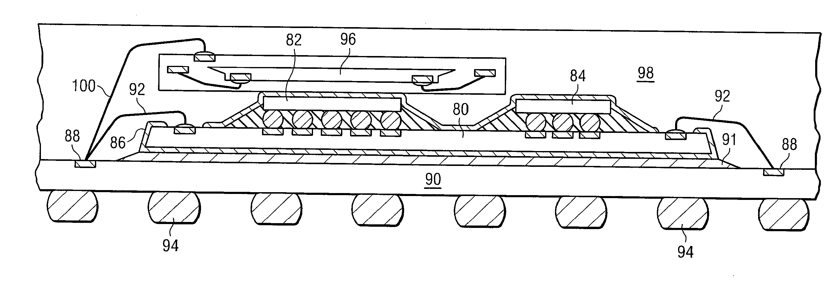
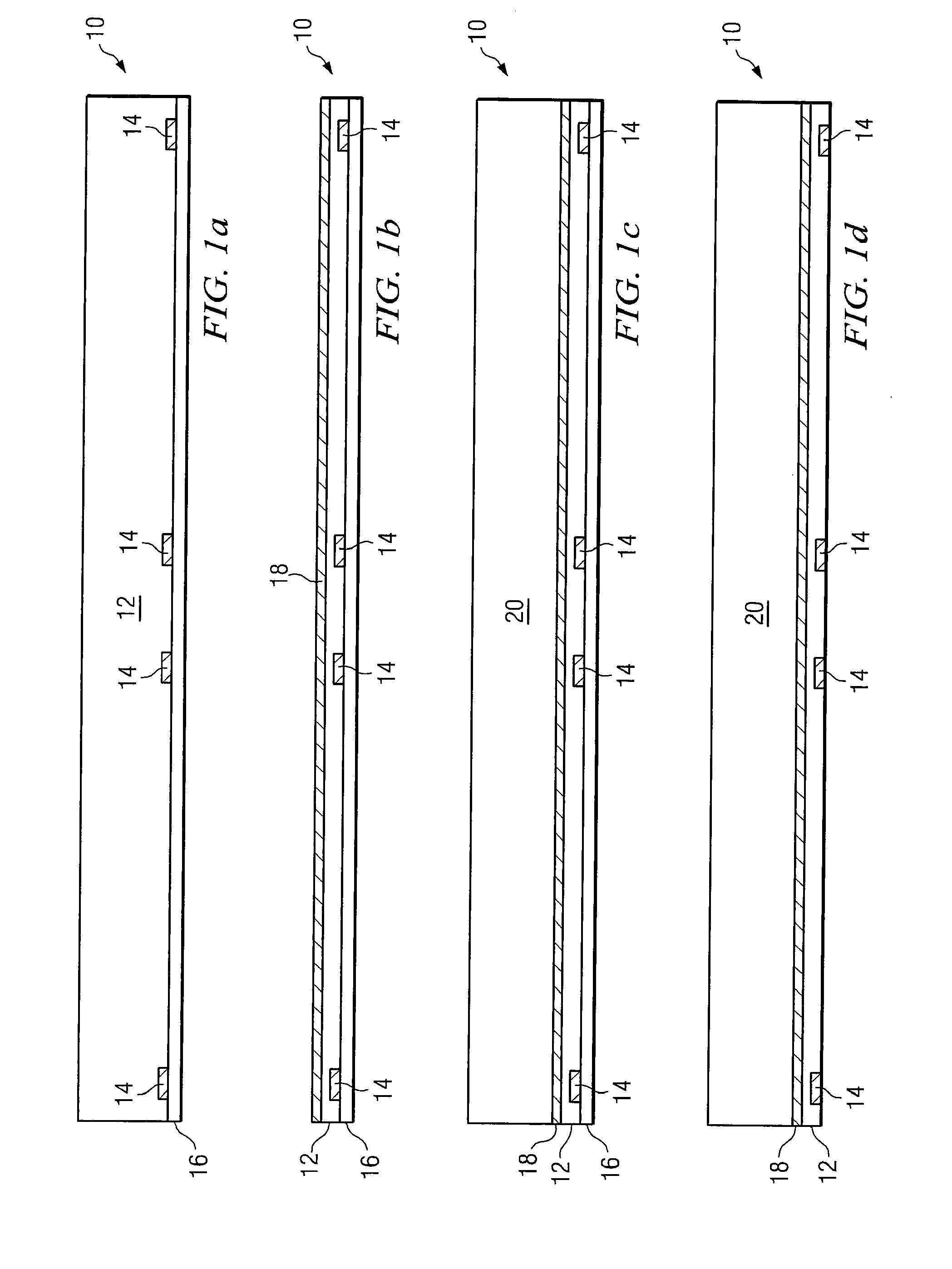
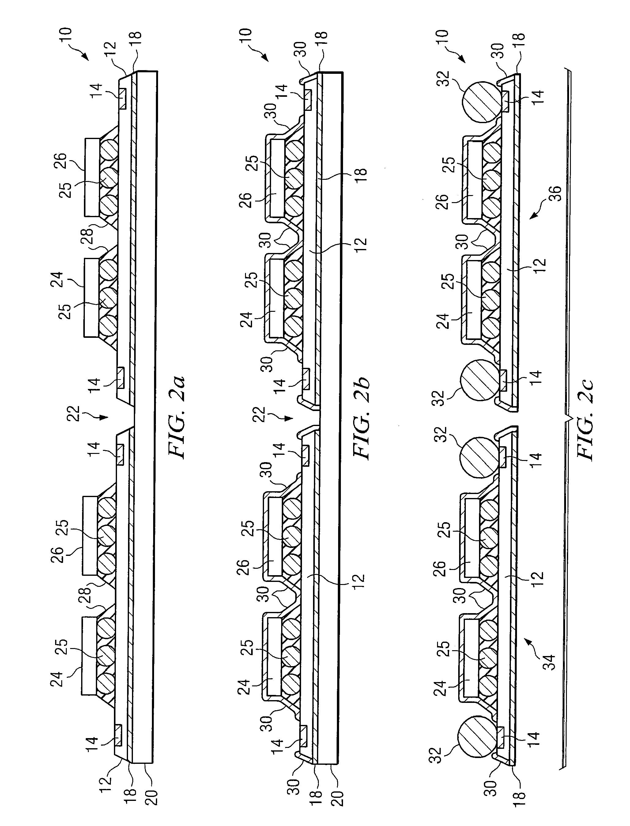
[0018]The present invention is described in one or more embodiments in the following description with reference to the Figures, in which like numerals represent the same or similar elements. While the invention is described in terms of the best mode for achieving the invention's objectives, it will be appreciated by those skilled in the art that it is intended to cover alternatives, modifications, and equivalents as may be included within the spirit and scope of the invention as defined by the appended claims and their equivalents as supported by the following disclosure and drawings.
[0019]The manufacture of semiconductor devices involves formation of a wafer having a plurality of die. Each die contains hundreds or thousands of transistors and other active and passive devices performing one or more electrical functions. For a given wafer, each die from the wafer typically performs the same electrical function. Front-end manufacturing generally ref...
PUM
 Abstract
Description
Claims
Application Information
 - R&D Engineer
- R&D Manager
- IP Professional
- Industry Leading Data Capabilities
- Powerful AI technology
- Patent DNA Extraction
Browse by: Latest US Patents, China's latest patents, Technical Efficacy Thesaurus, Application Domain, Technology Topic.
© 2024 PatSnap. All rights reserved.Legal|Privacy policy|Modern Slavery Act Transparency Statement|Sitemap