Measuring apparatus, exposure apparatus, and device fabrication method

a technology of exposure apparatus and measurement apparatus, which is applied in the direction of photomechanical apparatus, instruments, printing, etc., can solve the problems of increasing focus accuracy, non-negligible measurement errors attributed to the performance of an optical system which forms the surface position detection unit, and the inability to accurately measure the depth of focus. to achieve the effect of reducing the influence of optical system aberration and high accuracy

Inactive Publication Date: 2009-04-09
CANON KK
View PDF7 Cites 28 Cited by
  • Summary
  • Abstract
  • Description
  • Claims
  • Application Information

AI Technical Summary

Benefits of technology

[0014]The present invention provides a measuring apparatus which can measure the shape of a measurement target object with high accuracy by reducing the influence of the aberration of an optical system and that of a change in spectroscopic characteristics attributed to the transmittance of a glass material.

Problems solved by technology

However, in recent years, along with the shortening of the exposure light and an increase in the NA of the projection optical system, the depth of focus is becoming very small and therefore the accuracy of matching the surface of a substrate to be exposed with an optimal imaging position, that is, the so-called focus accuracy is increasingly becoming stricter.
More specifically, measurement errors attributed to the performance of an optical system which forms the surface position detection unit are becoming non-negligible in the surface position detection unit.
However, the technique disclosed in U.S. Pat. No. 6,249,351 measures the shape of a measurement target object corresponding to a wafer with an error due to the influence of the optical imaging performance of an optical system formed from lenses which are inserted between the measurement target object and an image sensing device, and adjust the measurement target object and the image sensing device to have an imaging relationship.
Such distortion of the interference signal generates an error in the measurement value of the substrate shape profile.
However, a broadband light source is desirably used to obtain a white light interference signal, so it is very difficult to decrease the aberration of the optical system.
Even when an optical system having a small aberration can be attained by increasing the number of lenses of the optical system or using an expensive glass material for the optical system, this entails a significantly high cost.
In this case, the transmittance on the short-wavelength side is often relatively low depending on the glass material used, which may exert an adverse influence on the interference signal.
Referring to the interference signal in case 4, light components in the short-wavelength range are absorbed so that a desired low coherency may not be obtained, resulting in the generation of an error in the measurement value of the substrate shape profile.
When this occurs, depending on the time taken to irradiate the measurement target object with light, the spectroscopic characteristics of a light component reflected by a reference surface and those of a light component reflected by the substrate surface change, resulting in the generation of an error in the measurement value of the substrate shape profile.

Method used


Image

  • Measuring apparatus, exposure apparatus, and device fabrication method
  • Measuring apparatus, exposure apparatus, and device fabrication method
  • Measuring apparatus, exposure apparatus, and device fabrication method

Examples


Embodiment Construction

[0035]A preferred embodiment of the present invention will be described below with reference to the accompanying drawings. The same reference numerals denote the same members throughout the drawings, and a repetitive description thereof will not be given.

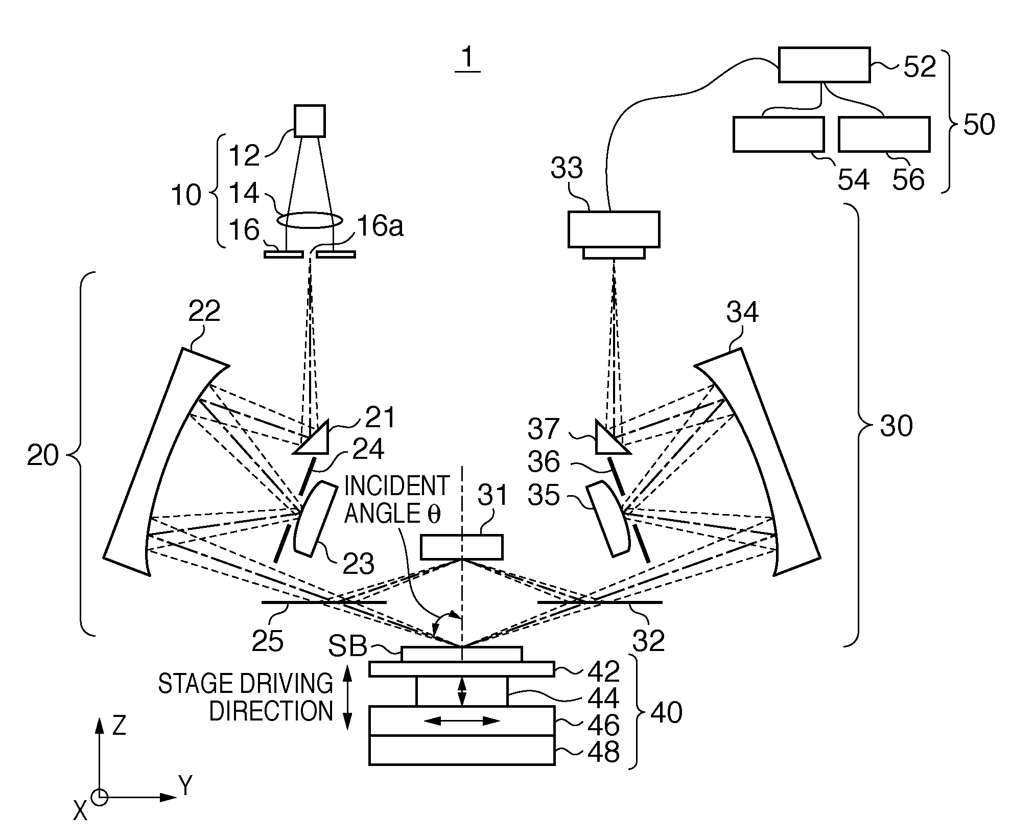
[0036]FIG. 1 is a schematic view showing the arrangement of a measuring apparatus 1 according to one aspect of the present invention. The measuring apparatus 1 measures the height information (Z position) of a substrate SB as the measurement target object at each point on the X-Y plane, and the average height information and average tilt information (ωx and ωy) of a predetermined region on the substrate SB. In other words, the measuring apparatus 1 measures the surface shape of the substrate SB as the measurement target object. When a plurality of thin films are formed on the substrate SB, the measuring apparatus 1 also measures the height information of the uppermost thin-film surface, the interface between each adjacent pair of th...


PUM


Abstract

The present invention provides a measuring apparatus which measures a shape of a surface of a measurement target object, comprising a light projecting optical system configured to split light from a light source into measurement light and reference light so that the measurement light enters the surface of the measurement target object and the reference light enters a reference mirror, a light receiving optical system configured to guide the measurement light reflected by the surface of the measurement target object and the reference light reflected by the reference mirror to a photoelectric conversion device, and a processing unit configured to calculate the shape of the surface of the measurement target object based on an interference pattern which is detected by the photoelectric conversion device and formed by the measurement light and the reference light.

Description

BACKGROUND OF THE INVENTION[0001]1. Field of the Invention[0002]The present invention relates to a measuring apparatus, an exposure apparatus, and a device fabrication method.[0003]2. Description of the Related Art[0004]A projection exposure apparatus has conventionally been employed to fabricate a micropatterned semiconductor device such as a semiconductor memory or logic circuit or a liquid crystal device by using photolithography. The projection exposure apparatus projects and transfers a pattern formed on a reticle (mask) onto a substrate such as a wafer by a projection optical system.[0005]Along with advance in micropatterning and an increase in packing density of semiconductor devices, the projection optical system is required to project and transfer the pattern of a reticle onto a substrate by exposure with a higher resolution. A minimum line width (resolution) that the projection exposure apparatus can transfer is proportional to the wavelength of light for use in exposure (...

Claims


Application Information

Patent Timeline
Patent Type & Authority Applications(United States)
IPC IPC(8): G01B11/02G03B27/42
CPCB82Y10/00B82Y40/00G01B11/2441G03F9/7049G03F9/7003G03F9/7026G03F7/0002
Inventor SASAKI, RYO
Owner CANON KK
Why Eureka
Try Eureka