
Method of inspecting semiconductor circuit having logic circuit as inspection circuit

Inactive Publication Date: 2009-04-16
ELPIDA MEMORY INC
View PDF12 Cites 8 Cited by
  • Summary
  • Abstract
  • Description
  • Claims
  • Application Information

AI Technical Summary

Benefits of technology

[0011]The present invention seeks to solve one or more of the ab

Problems solved by technology

With reduction of a semiconductor circuit, there is a problem that a test is restricted with respect to physical elements of a semiconductor testing apparatus (an LSI tester) for testing the semiconductor circuit.
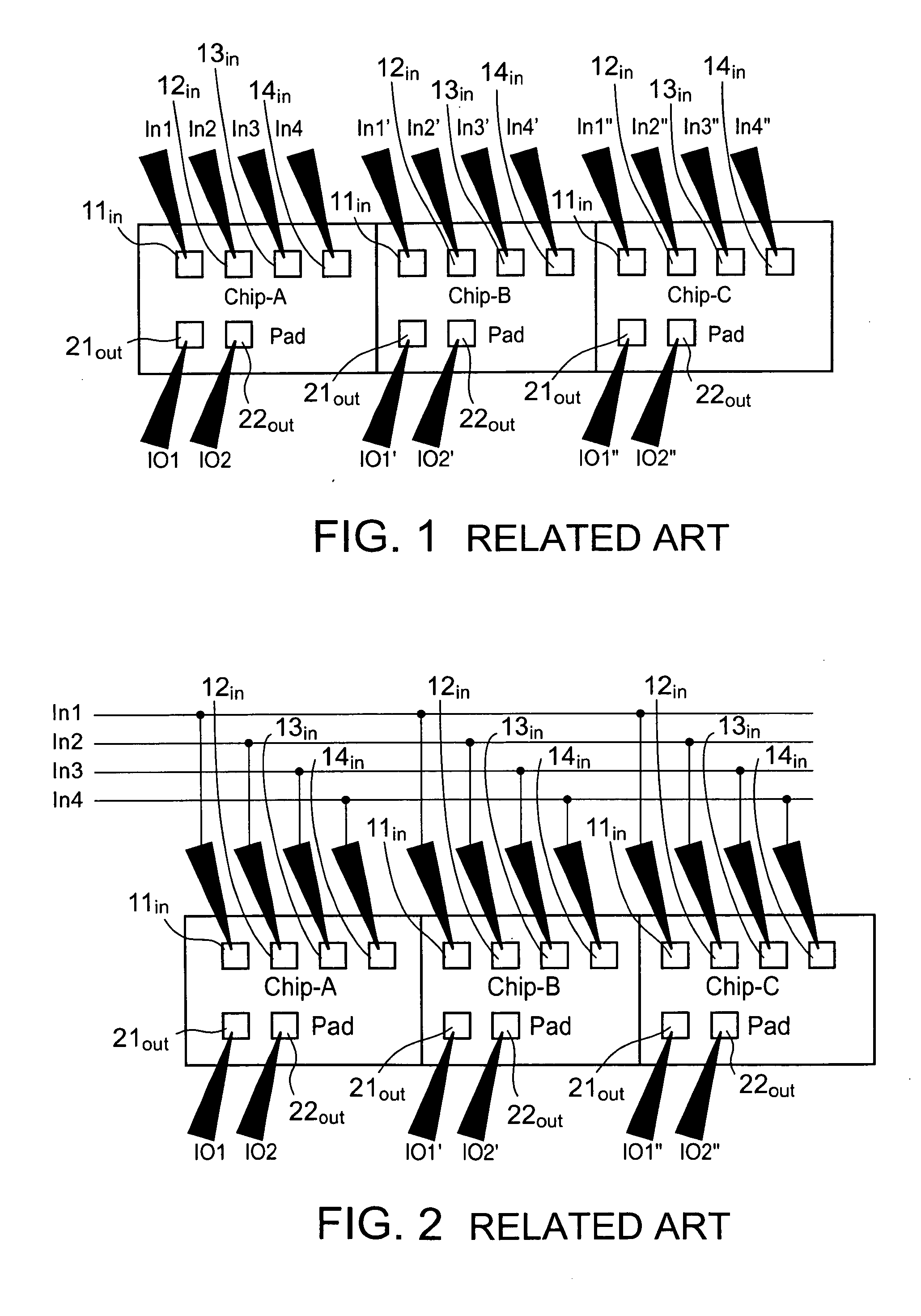
Herein, in a case of testing the semiconductor circuit, to test only one semiconductor circuit very reduces efficiency.
Furthermore, the Patent Document 1 neither discloses nor teaches technique for inspecting open (bonding failure) in a plurality of input terminals at a time.
Furthermore, it is impossible to test the semiconductor device at a time because the semiconductor circuits are selected by the selection signal in turn.

Method used


Image

  • Method of inspecting semiconductor circuit having logic circuit as inspection circuit
  • Method of inspecting semiconductor circuit having logic circuit as inspection circuit
  • Method of inspecting semiconductor circuit having logic circuit as inspection circuit

Examples


first embodiment

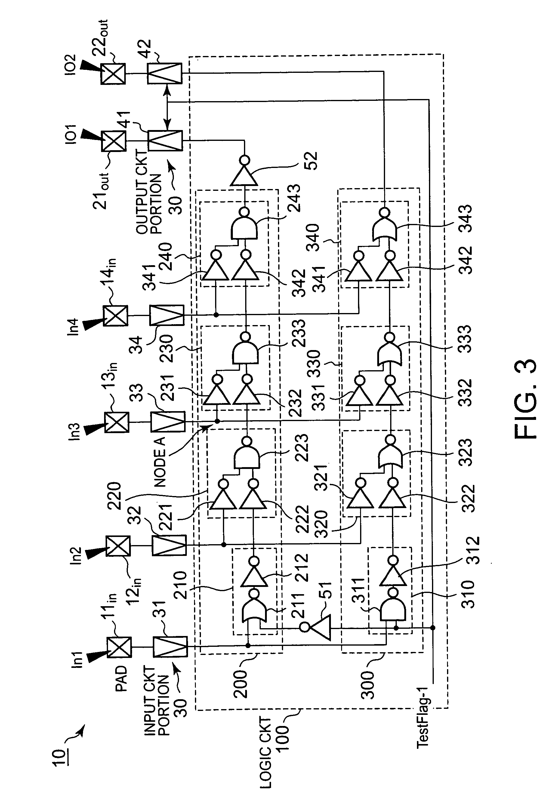
[0032]Referring to FIG. 3, the description will proceed to a semiconductor circuit 10 according to the present invention. FIG. 3 illustrates a part of an input circuit of the semiconductor circuit 10 and shows an example which uses a logic circuit 100 as an inspection circuit of the semiconductor circuit 10.

[0033]In general, in the manner which is described above, the semiconductor circuit has first through N-th input terminals and first through M-th output terminals (input / output terminals), where each of N and M represents an integer which is not less than two. Herein, in order to simplify the description, the description will be exemplified in a case where the integer N is equal to four and the integer M is equal to two.

[0034]The illustrated semiconductor circuit 10 has first through fourth input terminals 11in, 12in, 13in and 14in and first and second output terminals 21out and 22out. The first through the fourth input terminals 11in to 14in are connected to first through fourth...

second embodiment

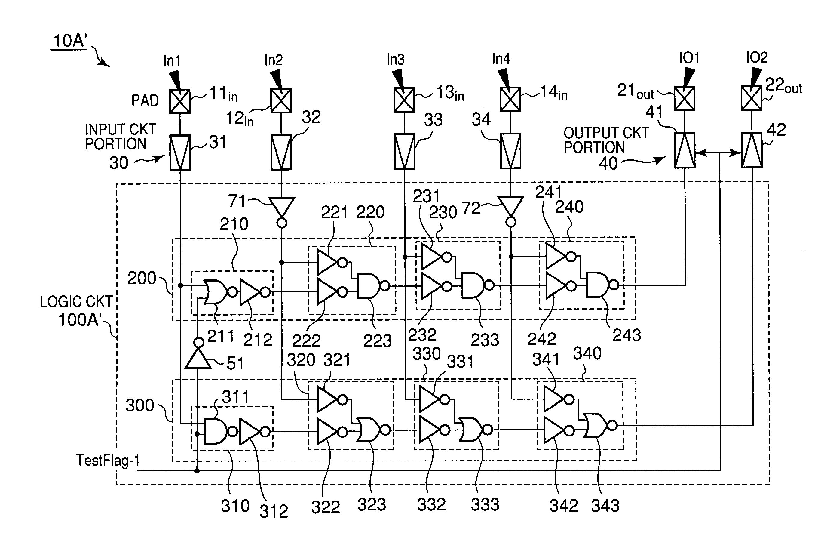
[0078]Referring to FIG. 5, the description will proceed to a semiconductor circuit 10A according to the present invention. FIG. 5 illustrates a part of an input circuit of the semiconductor circuit 10A and shows an example which uses a logic circuit 100A as an inspection circuit of the semiconductor circuit 10A.

[0079]The illustrated logic circuit 100A is similar in structure and operation to the logic circuit 100 illustrated in FIG. 3 except that first and second inverters 71 and 72 are added thereto. Components having structure similar to those illustrated in FIG. 3 are depicted at similar reference symbols and only different points will be described in order to simplify the description.

[0080]The first inverter 71 is inserted between the second input buffer 32 and the one input port of the second OR circuit 220 in the OR circuit portion 200. In other words, supplied to the second input terminal 12in, the input signal is supplied to the first inverter 71 through the second input buf...


PUM


Abstract

A semiconductor circuit includes an inspection circuit for inspecting terminal open of the semiconductor circuit. The semiconductor circuit has a plurality of input terminals. The semiconductor circuit includes an input circuit portion connected to the plurality of input terminals. The inspection circuit includes a logic circuit, supplied with a plurality of input signals from the input circuit portion, for performing a predetermined logic operation to the plurality of input signals to produce a logic operation result. Whereby the semiconductor circuit enables to decide the presence or absence of the terminal open on the basis of the logic operation result.

Description

[0001]This application is based upon and claims the benefit of priority from Japanese patent application No. 2007-264025, filed on Oct. 10, 2007, the disclosure of which is incorporated herein in its entirety by reference.BACKGROUND OF THE INVENTION[0002]1. Field of the Invention[0003]This invention relates to a semiconductor circuit and a method of inspecting the same.[0004]2. Description of Related Art[0005]With reduction of a semiconductor circuit, there is a problem that a test is restricted with respect to physical elements of a semiconductor testing apparatus (an LSI tester) for testing the semiconductor circuit. Although it is measures directed toward the improvement of measurement efficiency, in recent years, it becomes required to divert defective items with reliability.[0006]Herein, in a case of testing the semiconductor circuit, to test only one semiconductor circuit very reduces efficiency. As a result, parallel (concurrently) test is carried out with a plurality of semi...

Claims


Application Information

Patent Timeline
IPC IPC(8): G01R31/02H03K19/00
CPCG01R31/31715
Inventor KOYAMA, TAKAHIRO
Owner ELPIDA MEMORY INC
Learn More