

Film forming apparatus and method, gas supply device and storage medium
Active Publication Date: 2009-04-23
TOKYO ELECTRON LTD
View PDF32 Cites 307 Cited by
- Summary
- Abstract
- Description
- Claims
- Application Information
AI Technical Summary
Benefits of technology
[0013]In accordance with the above characteristics, the cooling operation of the cooling unit is directly applied to the shower head, so that responsiveness in cooling is good. That is, the temperat
Problems solved by technology
However, when the temperature of the heater of the stage increases, a temperature of a shower head surface which comes in contact with the processing space increases by heat radiated from the heater of the stage during the film forming process.
Moreover, due to the temperature increase, the film is more easily adhered to the shower head, and the temperature of the shower head increases even further, leading to a vicious cycle.
As a result, it is not possible to perform the temperature control by the heater provided on the side of the shower head.
That is, the temperature control of the shower head which is required in the film forming process may not be performed.
Further, when the sho
Method used
View moreImage
Smart ImageViewing Examples

Examples
 PUM
| Property | Measurement | Unit |
|---|---|---|
| Temperature | aaaaa | aaaaa |
Abstract
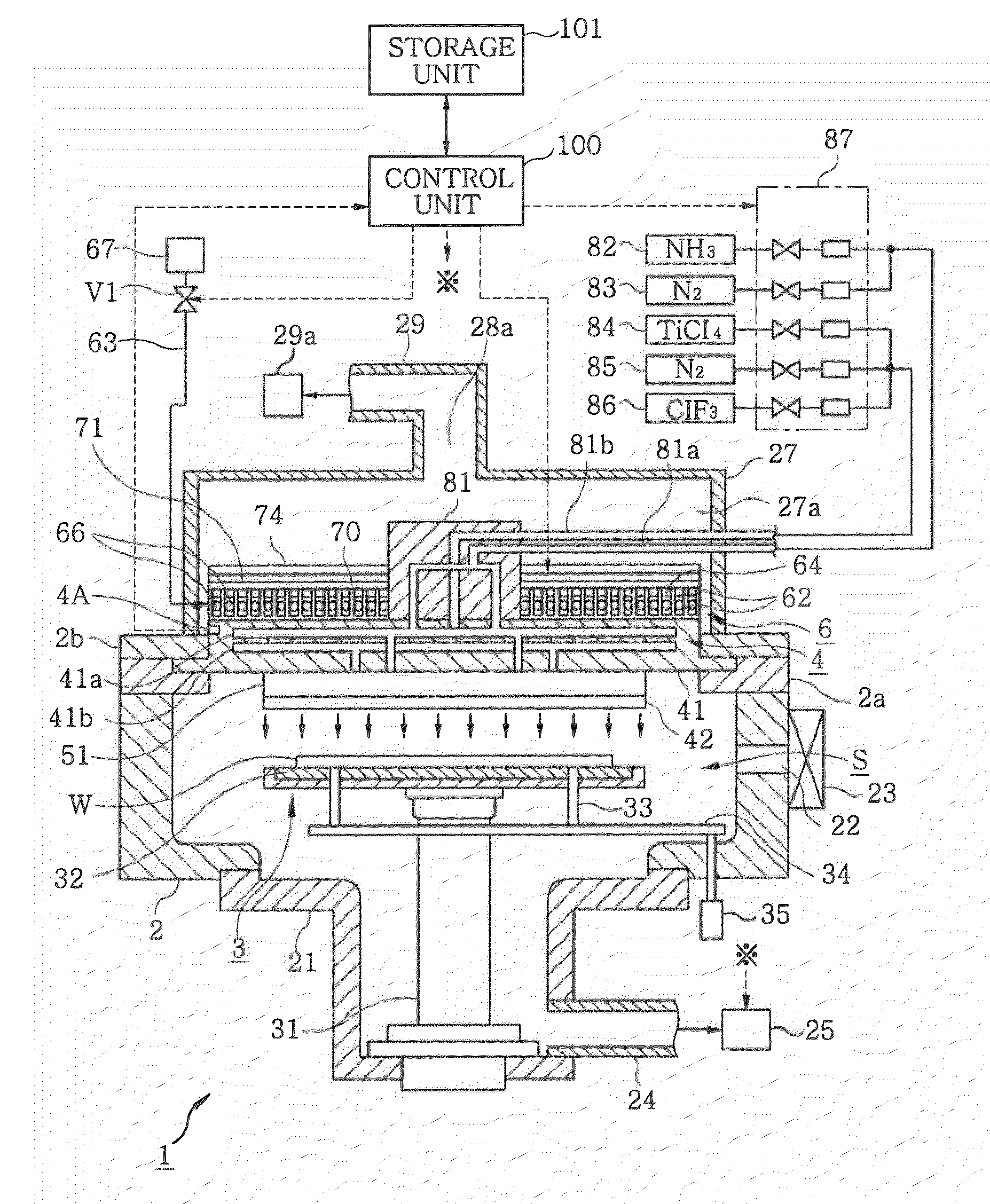
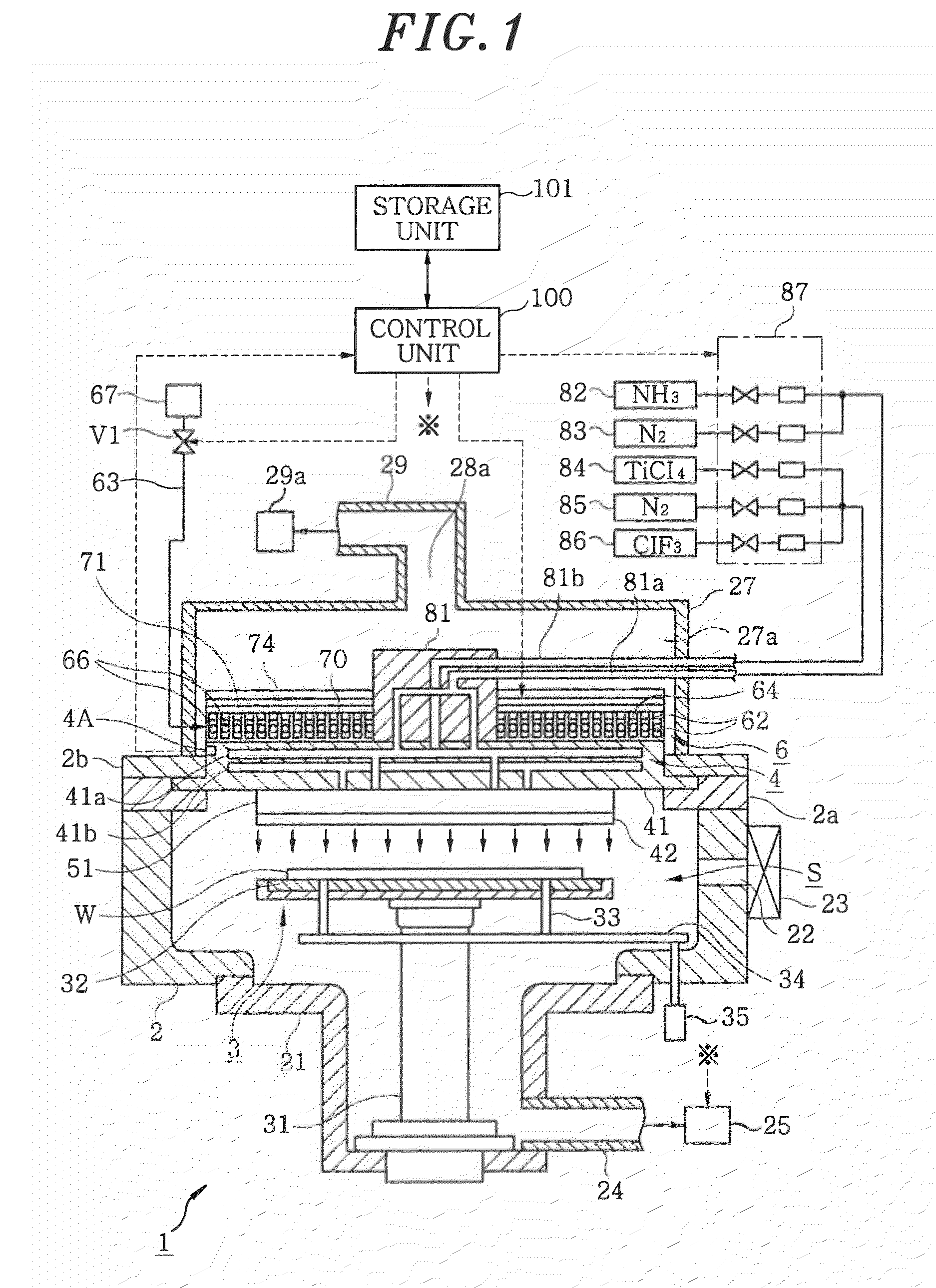
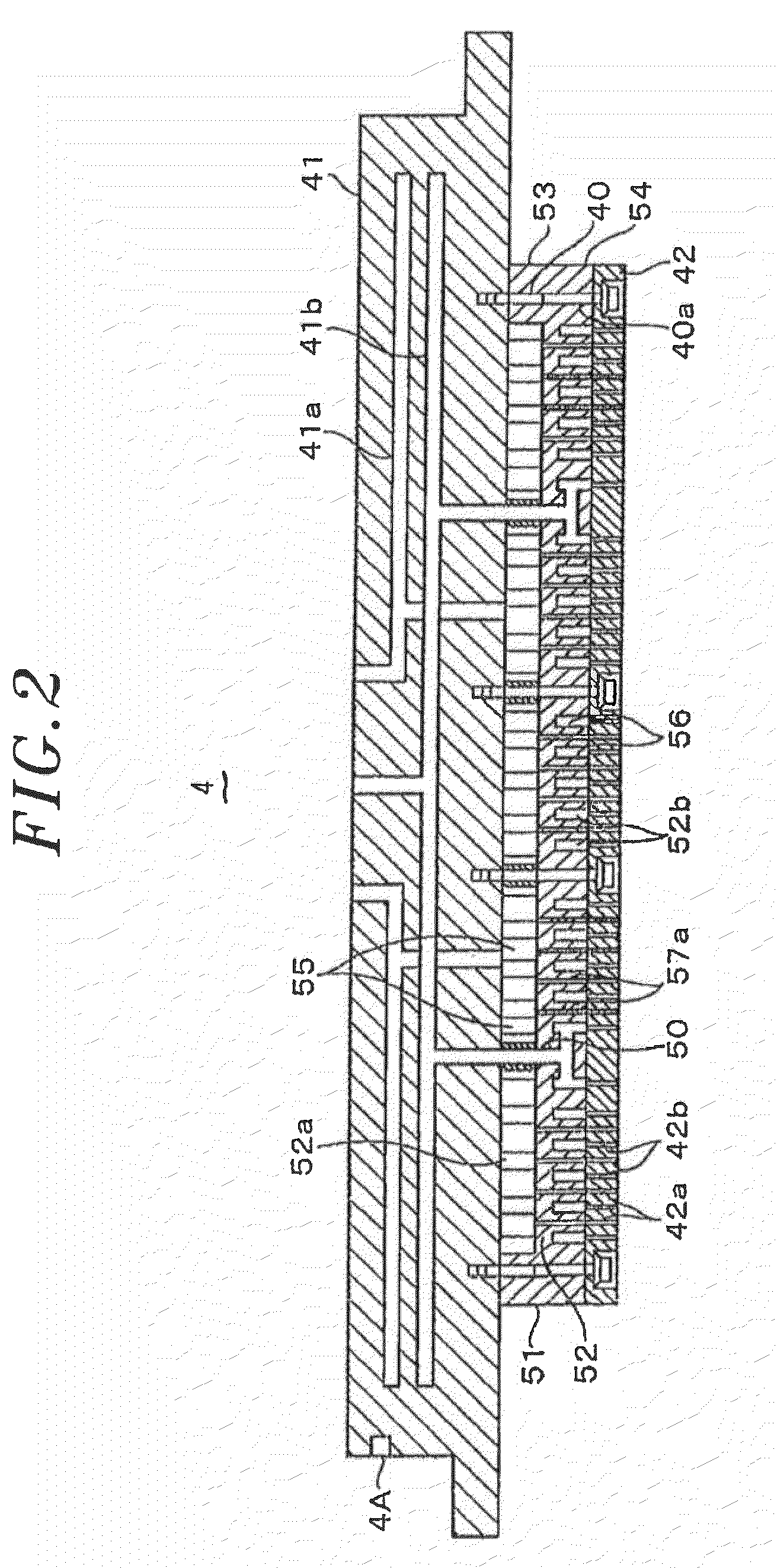
A film forming apparatus is provided with a chamber which defines a processing space for performing a film forming process to a substrate a stage arranged in the chamber for mounting the substrate thereon; a substrate heating unit arranged on the stage for heating the substrate; a shower head which is arranged to face the stage and has many gas injecting holes; a gas supply unit for supplying cooling unit arranged above the shower head for cooling the shower head; and a shower head heating unit arranged above the cooling unit for heating the shower head through the cooling unit.
Description
[0001]This application is a Continuation Application of PCT International Application No. PCT / JP2007 / 062328 filed on Jun. 19, 2007, which designated the United States.FIELD OF THE INVENTION[0002]The present invention relates to a film forming apparatus and method for forming a predetermined thin film on a substrate by a chemical vapor deposition (CVD) method.BACKGROUND OF THE INVENTION[0003]In a semiconductor manufacturing process, in order to fill holes between wirings formed on a semiconductor wafer as a substrate to be processed (hereinafter, referred to as a “wafer”), or in order to provide a barrier layer, a thin film is formed by depositing a metal such as Ti, Al, Cu or the like or a metal compound such as WSi, TiN, TiSi or the like. Such thin film of the metal or metal compound is formed by means of a CVD method which has a better buriability compared to a physical vapor deposition (PVD) method.[0004]A CVD film forming apparatus includes: a wafer stage provided in a chamber a...
Claims
Login to View More Application Information
Patent Timeline
 IPC IPC(8): C23C16/44C23C16/54
CPCC23C16/34C23C16/45523C23C16/4557H01L21/76841C23C16/45574H01L21/28562H01L21/67109C23C16/45572H01L21/205
InventorKAKEGAWA, TAKASHI
OwnerTOKYO ELECTRON LTD