RFID antenna system and method

a technology of rfid antenna and antenna system, which is applied in the field of radio frequency identification (“ rfid”) communication, can solve the problems of reducing the operating range of an interrogator, and reducing the efficiency of the rfid power transfer

Inactive Publication Date: 2009-04-30
SENSORMATIC ELECTRONICS CORP
View PDF18 Cites 66 Cited by
  • Summary
  • Abstract
  • Description
  • Claims
  • Application Information

AI Technical Summary

Problems solved by technology

While technology exists to drastically reduce the size of an IC component of an RFID device, similar miniaturization of the antenna of an RFID device can result in a significant reduction in performance.
By reducing the overall size of the RFID device, and thus the antenna, it may prove difficult to adequately provide the impedance characteristics for efficient function of the device.
As such, the RFID may suffer from inefficient power transfer to the IC, a reduced operating range with respect to an interrogator, and a weak return signal in response.
Other substrates may cause the radiation efficiency of the antenna to deteriorate from the designed optimal mounting substrates.
Thus, the antenna, and consequently the RFID device, will no longer function as intended.
This loss of antenna efficiency may be due to a number of variable packaging factors.
Impedance matching ensures the most efficient energy transfer between an antenna and the wireless communication device, as discussed above, and placement of an RFID device in proximity to a surface having dielectric and conductive properties outside of a particular range may reduce the performance of the RFID device.
These adverse effects to the performance of an RFID device may also be experienced upon the inclusion or integration of an electronic article surveillance (“EAS”) tag or device.
Such EAS devices often include a magneto-acoustic mechanism having one or more metallic components that may subsequently interfere with or reduce the performance characteristics of a particular RFID device.

Method used


Image

  • RFID antenna system and method
  • RFID antenna system and method
  • RFID antenna system and method

Examples


Embodiment Construction

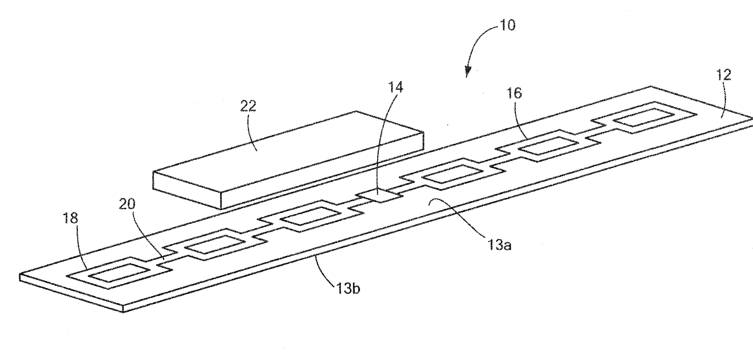
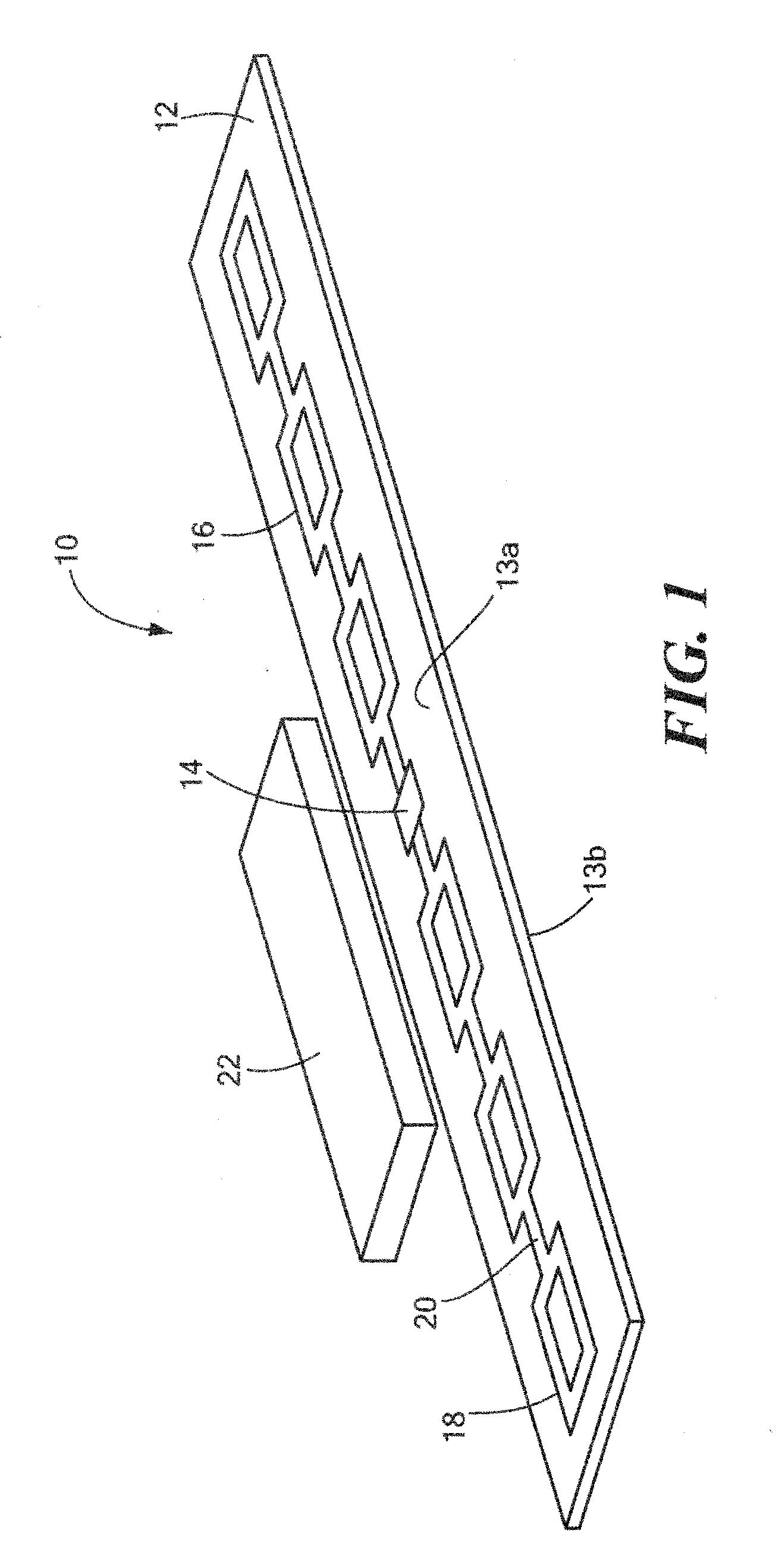
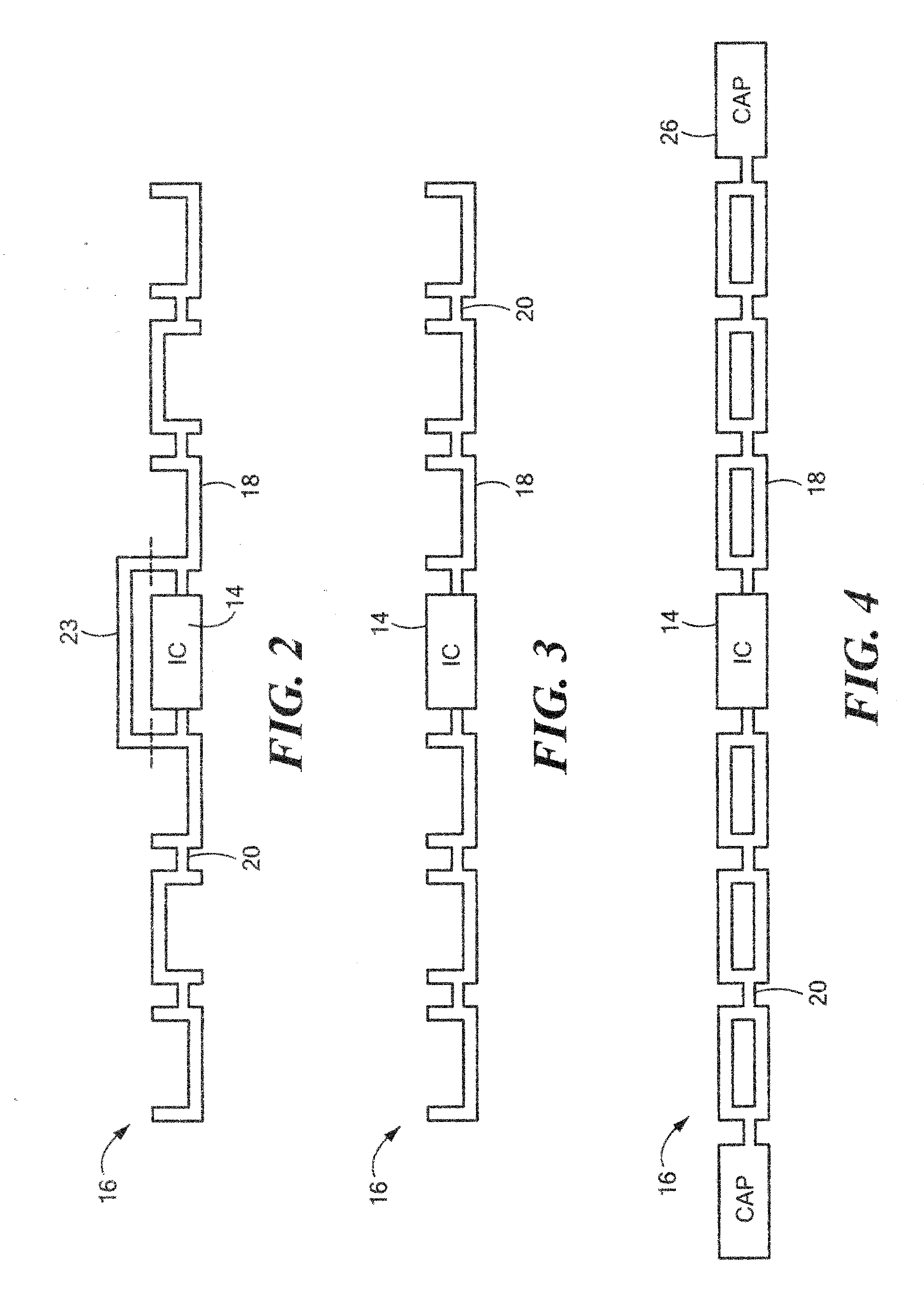
[0021]Referring now to the drawing figures in which like reference designators refer to like elements, there is shown in FIG. 1 a diagram of an exemplary apparatus constructed in accordance with the principles of the present invention and designated generally as “10”. Apparatus 10 is an RFID device that may generally include a substrate body 12, with an integrated circuit (“IC”) component 14 coupled to the substrate body 12, as well as an antenna 16 disposed on the substrate body 12 in electrical communication with the IC component 14. Antenna 16 may generally include a pattern of conductive material. In particular, the antenna 16 may include a plurality of substantially square or rectangular shaped polygons 18 having squared or rounder corners, where a portion of the polygons 18 are hollowed out, i.e., do not contain a conductive material. The plurality of polygons 18 may be electrically coupled to one another by a strip or portion of conductive material 20 connecting each polygon ...


PUM


Abstract

The present invention provides an RFID device having a substrate body, and an IC component and antenna disposed thereon. The RFID device may further include one or more spacing elements, wherein at least a portion of the substrate body is adapted to be disposed around at least a portion the spacing element, thus reducing the overall size of the substrate body with proper impedance matching. The RFID device may further include an EAS element coupled to the substrate body and / or the spacing element in order to create a combination RFID / EAS device with the ability to reduce its overall footprint without sacrificing the ability to provide both identification and article surveillance functions.

Description

CROSS-REFERENCE TO RELATED APPLICATION[0001]Not Applicable.STATEMENT REGARDING FEDERALLY SPONSORED RESEARCH OR DEVELOPMENT[0002]Not ApplicableFIELD OF THE INVENTION[0003]The present invention relates to the field of radio frequency identification (“RFID”) communications, and in particular towards RFID transponder configurations.BACKGROUND OF THE INVENTION[0004]Radio frequency identification (RFID) devices are becoming increasingly popular for a variety of industrial, retail, transportation, and other applications. RFID technology provides a positive identity for any object, person, or the like, bearing an RFID transponder through the use of a passive, radio frequency signal. In a typical application, an RFID transponder comprises an antenna and an integrated circuit. When a separate RFID reading device broadcasts a radio frequency signal, the signal interacts with the RFID transponder antenna. The transponder antenna converts part of the received RF signal energy into an electrical ...

Claims


Application Information

Patent Timeline
Patent Type & Authority Applications(United States)
IPC IPC(8): H04B7/00H01L21/02
CPCH01Q1/2225G06K19/07749G06K19/07786G08B13/2417G08B13/2437H01Q9/285
Inventor DAY, EDWARD
Owner SENSORMATIC ELECTRONICS CORP
Why Eureka
Try Eureka