Multiple package module using a rigid flex printed circuit board

Inactive Publication Date: 2009-04-30
CHIPSTACK
View PDF16 Cites 6 Cited by
  • Summary
  • Abstract
  • Description
  • Claims
  • Application Information

AI Technical Summary

Problems solved by technology

Such custom design of each circuit board for each particular application increases the cost of creating a line of products.
The key components may be electrically sensitive, difficult to fabricate, a specified circuit and the like.
Although an MPM provides design flexibility, an MPM decreases the connection complexity.
Mapping the various conductive traces from the MPM to the supporting circuit board can be tedious.
Providing solder connections between the many traces and the supporting circuit board using conductive vias is prone to connection failure.

Method used


Image

  • Multiple package module using a rigid flex printed circuit board
  • Multiple package module using a rigid flex printed circuit board
  • Multiple package module using a rigid flex printed circuit board

Examples


Embodiment Construction

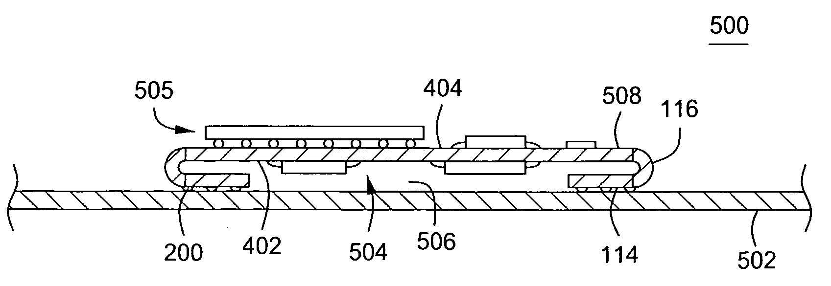
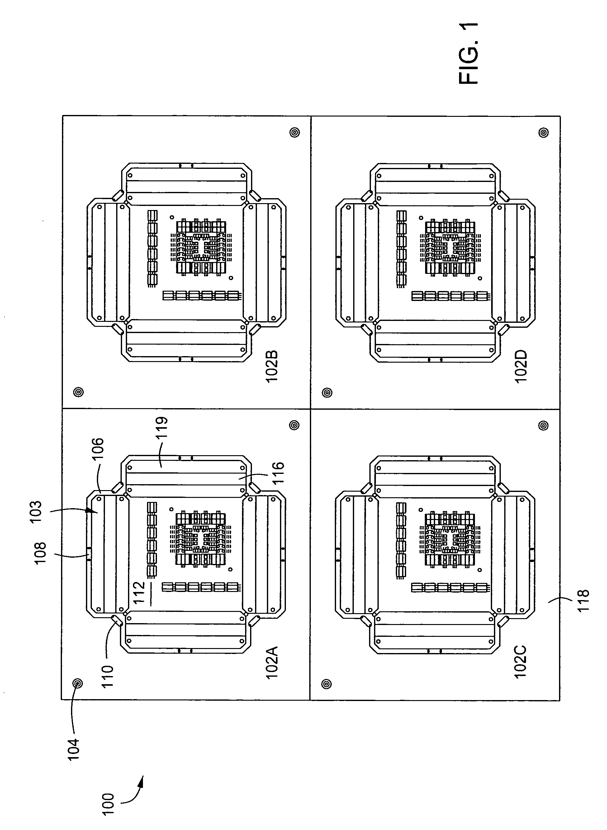
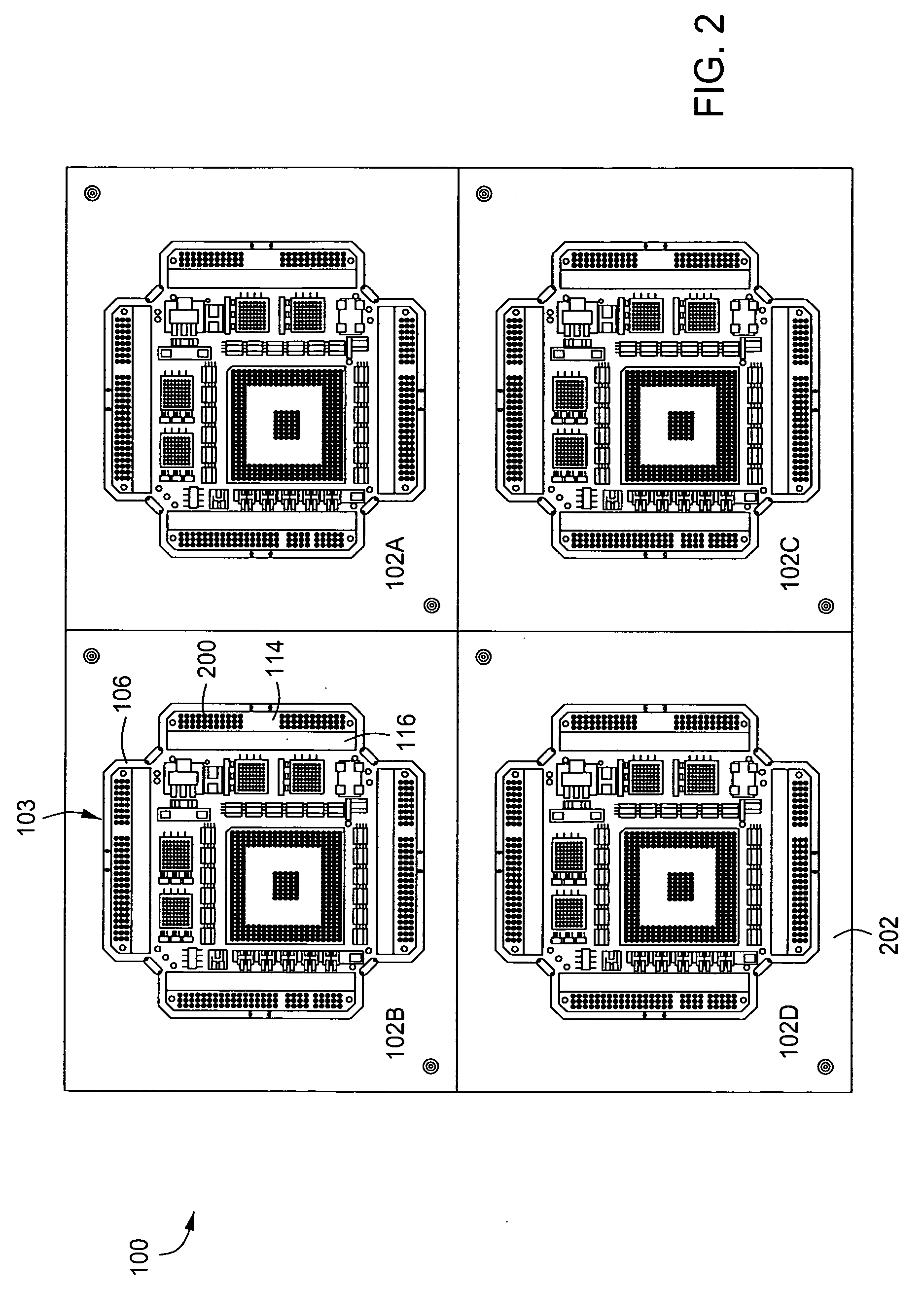
[0022]FIG. 1 depicts a top plan view of a first side 118 of a frame 100 within which a plurality of multiple package modules (MPM) rigid flex circuit boards 103 are fabricated. FIG. 2 depicts the second side 202 of the frame 100 comprising the plurality of rigid flex circuit boards for multiple package modules 103. To best understand the invention FIGS. 1 and 2 should be referred to simultaneously.

[0023]The frame 100 comprises a plurality of regions 102A, 102B, 102C, 102D wherein an MPM 103 is fabricated in a rigid flex circuit board. Apertures 104 are distributed upon each of the regions 102A, 102B, 102C, and 102D to facilitate alignment of individual circuits during assembly, test, rework. In one embodiment, the rigid flex circuit board can be fabricated in accordance with U.S. Pat. No. 5,499,444, entitled Method of Manufacturing a Rigid Flex Printed Circuit Board, issued Mar. 19, 1996, which is hereby incorporated by reference in its entirety. In another embodiment of the inventi...


PUM

PropertyMeasurementUnit
Flexibilityaaaaaaaaaa

Abstract

A multiple package module and a method of fabricating a multiple package module. The module comprises a central region of a rigid flex circuit board for mounting circuitry, and at least one wing connected by a flexible portion to at least one edge of the central region of the rigid flex circuit board.

Description

CROSS-REFERENCE TO RELATED APPLICATIONS[0001]This application claims benefit of U.S. Provisional Patent Application Ser. No. 61 / 000,337, filed Oct. 25, 2007, which is herein incorporated by reference.BACKGROUND OF THE INVENTION[0002]1. Field of the Invention[0003]Embodiments of the present invention generally relate to integrated circuit packaging and mounting and, more particularly, to multiple package modules (MPM) formed using a rigid flex printed circuit board.[0004]2. Description of the Related Art[0005]An important aspect of modern electronics packaging is increasing the component density. A compact packaging technology is needed when mounting area upon a circuit board is limited, dictating that circuit elements be closely spaced. Modules containing a number of semiconductor devices are used to densely place semiconductor devices (i.e., integrated circuits) and to obtain a small sized electronic device. In many applications, a large circuit board may be used within, for exampl...

Claims


Application Information

Patent Timeline
IPC IPC(8): H05K7/00H05K3/00
CPCH01L23/4985H01L25/0652H05K1/141H05K1/147Y10T29/49124H05K3/363H05K3/4691H05K2201/055H01L2224/16H05K1/148
Inventor ARNOLD, SHAWN
Owner CHIPSTACK
Why Eureka
Try Eureka