Method of manufacturing semiconductor device

a manufacturing method and semiconductor technology, applied in the direction of semiconductor devices, basic electric elements, electrical equipment, etc., can solve the problems of difficult to achieve a high breakdown voltage and increase costs

Active Publication Date: 2009-04-30
FUJI ELECTRIC CO LTD
View PDF2 Cites 7 Cited by
  • Summary
  • Abstract
  • Description
  • Claims
  • Application Information

AI Technical Summary

Benefits of technology

[0016]According to one aspect of the present invention, a method of forming a semiconductor, which can be a MOSFET or IGBT includes the steps of, forming a RESURF region of a second-conductivity type in one surface of a semiconductor layer of a first-conductivity type, wherein the RESURF region has an annular configuration, forming a plurality of trenches from the one surface of the semiconductor layer after forming the RESURF region, wherein each of the trenches has a striped configuration and a depth smaller than a diffusion depth of the RESURF region, and wherein the RESURF region surrounds the trenches with opposite longitudinal ends of each of the trenches overlapping portions of the RESURF region, forming trench gate electrodes in the trenches with a first insulating film interposed between each of the trench gate electrodes and the trenches after forming the trenches, and forming a well region of the second-conductivity type in the one surface of the semiconductor layer, wherein the well region intersects the RESURF region.
[0017]According to another aspect of the present invention, the method comprises the steps of, providing a semiconductor layer of a first-conductivity type, forming a first semiconductor region of a second-conductivity type in one surface of the semiconductor layer, wherein the first semiconductor region has an annular configuration, forming a plurality of trenches from the one surface of the semiconductor layer, wherein each of the trenches having a striped configuration and a depth smaller than a diffusion depth of the first semiconductor region, and wherein the first semiconductor region surrounds the trenches with opposite longitudinal ends of each of the trenches overlapping portions of the first semiconductor region, covering the trenches and portions of the first semiconductor region adjacent to the opposite longitudinal ends of the trenches with a first insulating film, covering an outer portion of the first semiconductor region and a portion of the semiconductor layer surrounding the first semiconductor region with a second insulating film that is thicker than the first insulating film, wherein the second insulating film is connected to the first insulating film, filling each of the trenches with a conductive material, with the first insulating film interposed in between, and covering part of the second insulating film with the conductive material.
[0018]The method further includes the steps of forming a second semiconductor region of the second-conductivity type in the one surface of the semiconductor layer using the conductive material as a mask, wherein an impurity concentration of the second semiconductor region is higher than that of the first semiconductor region, a diffusion depth of the second semiconductor region is smaller than the depth of the trenches, and an outer portion of the second semiconductor region coextends with an inner portion of the first semiconductor region.
[0019]The method further includes forming third semiconductor regions of the first-conductivity type in the one surface of the semiconductor layer, wherein the third semiconductor regions are formed adjacent to side surfaces of the trenches and extend along a longitudinal direction of the trenches, and wherein an impurity concentration of the third semiconductor regions is higher than the impurity concentration of the second semiconductor region.

Problems solved by technology

Where the n− semiconductor layer 1 is formed by epitaxial growth, this means cost increase.
Moreover, if the diffusion depth of the p-well region 10 is small, the electric field intensity is increased along the edge a, which makes it difficult to attain a high breakdown voltage.

Method used


Image

  • Method of manufacturing semiconductor device
  • Method of manufacturing semiconductor device
  • Method of manufacturing semiconductor device

Examples


Embodiment Construction

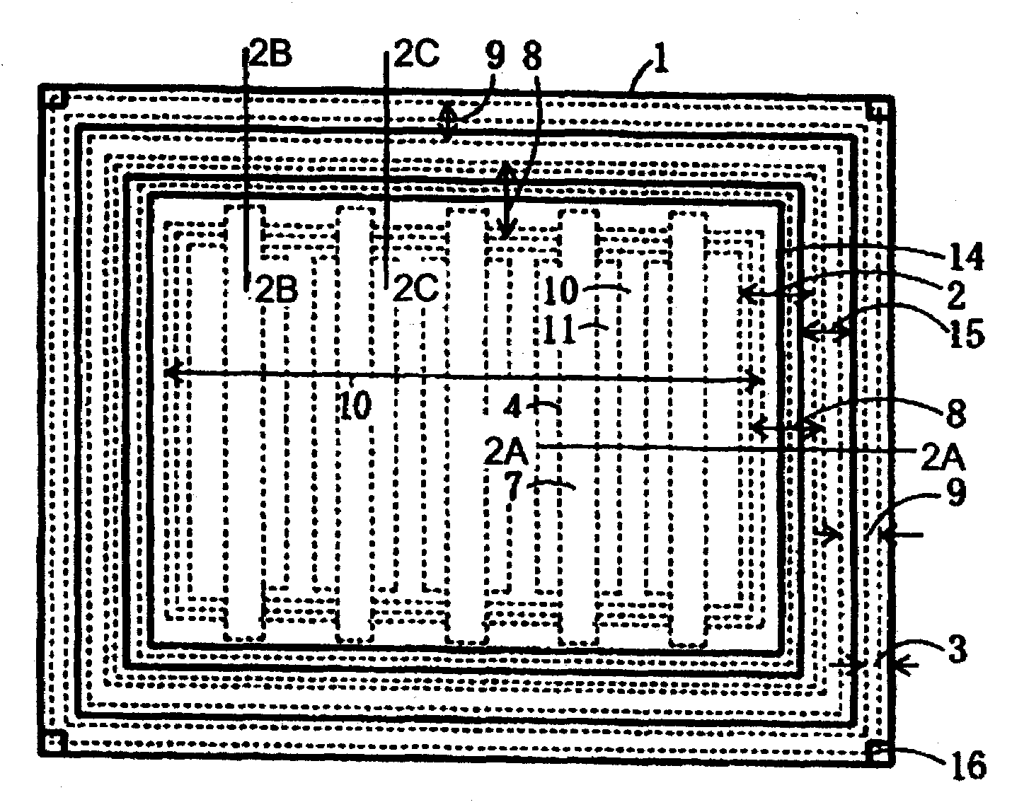
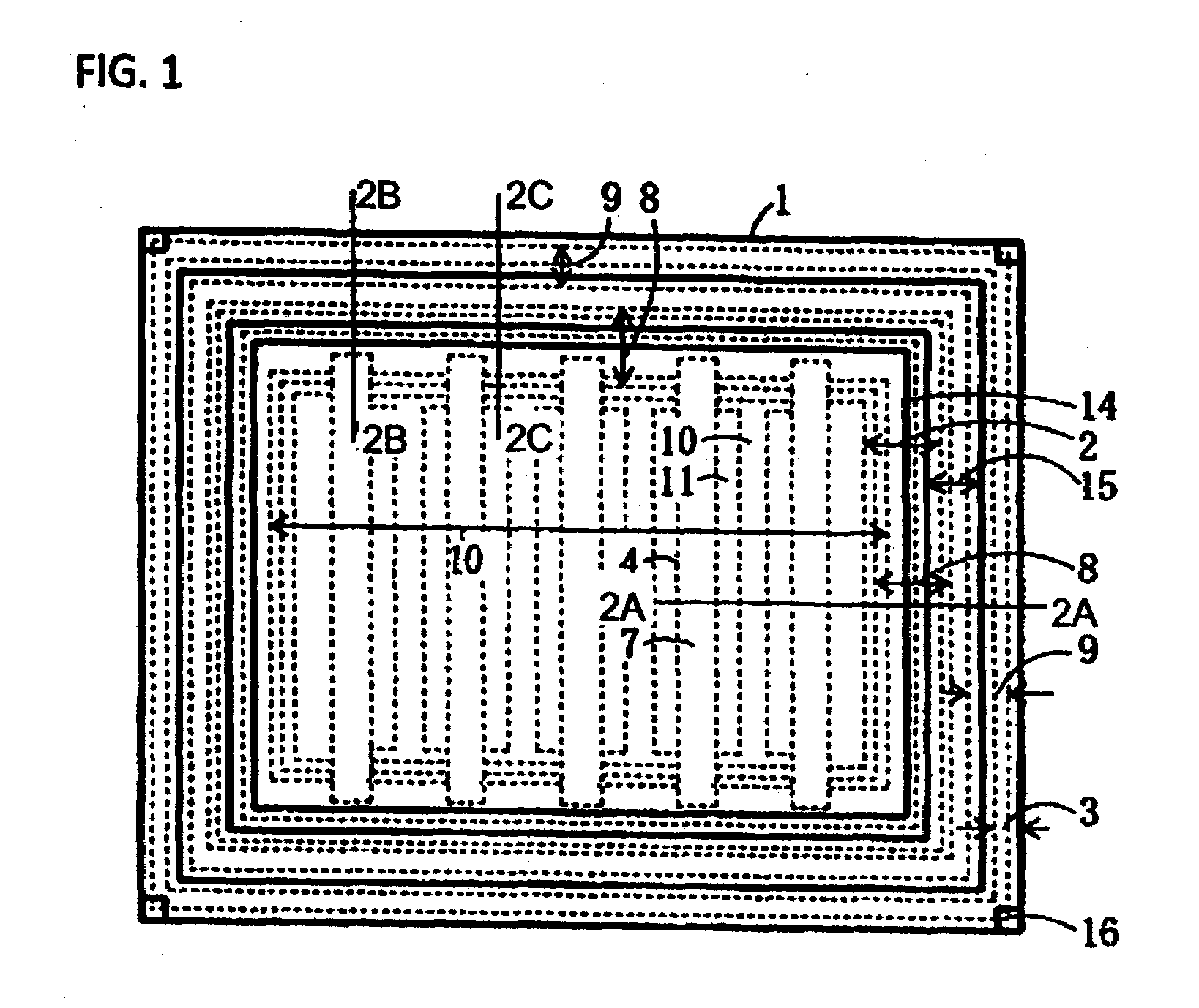
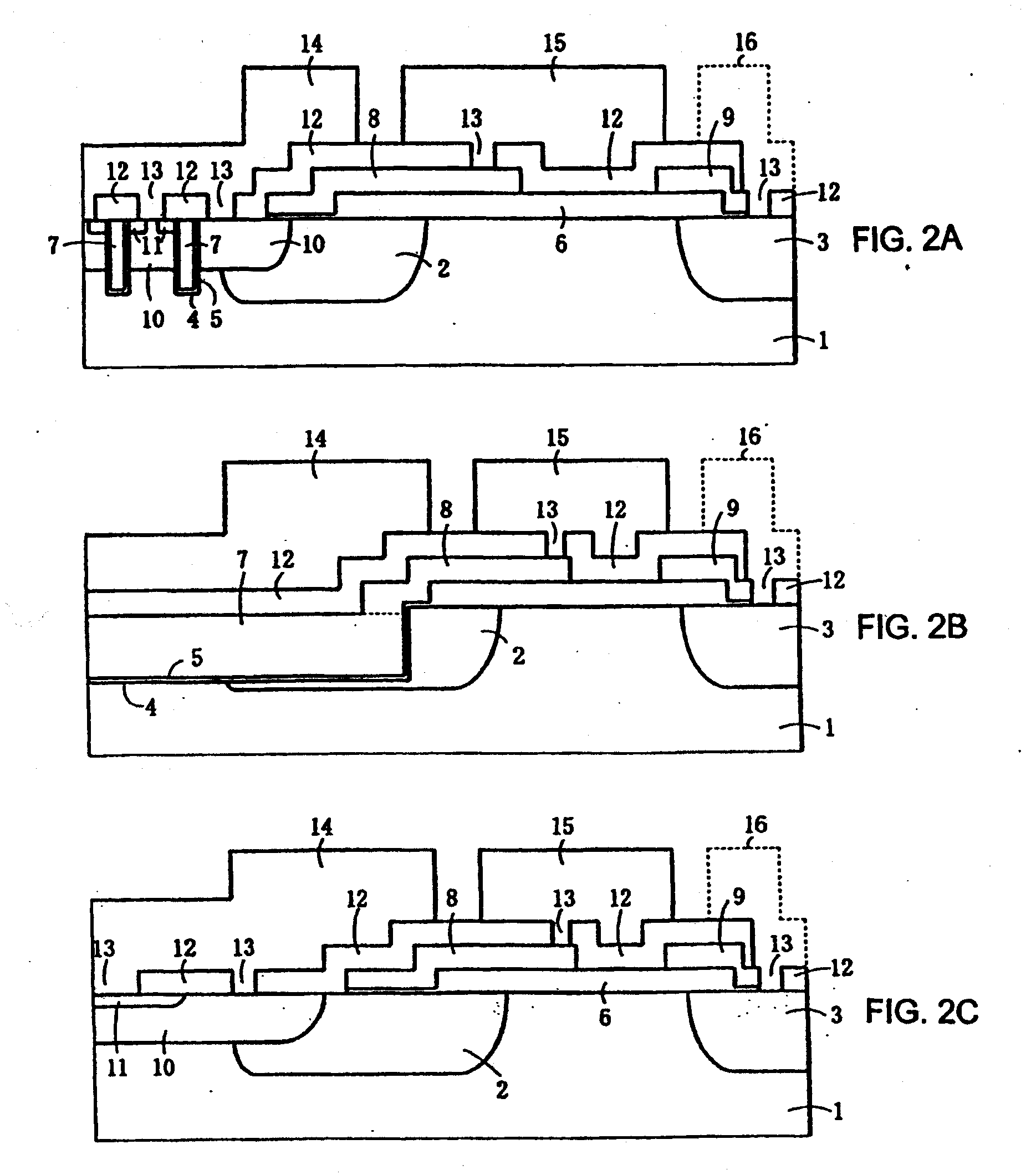
[0034]An embodiment of a semiconductor device, namely a vertical n-channel MOSFET having a trench gate structure, is described. Layers, regions, etc., corresponding to elements of the above-described conventional MOSFET are given the same reference symbols. Although in the embodiment described here refers the first conductivity type as the n type and the second conductivity type as the p-type, the conductivity types can be reversed. Superscripts “+” and “−” following “p” and “n” mean that the impurity concentration is high and low, respectively.

[0035]Referring to FIGS. 1 and 2A-2C, the vertical n-channel MOSFET having a trench gate structure includes an n− semiconductor layer 1 (n− drift layer) formed on an n+ semiconductor substrate (not shown), and layers, regions, etc. formed over or in the surface of the n− semiconductor layer 1. A vertical IGBT can be obtained by replacing the n+ semiconductor substrate (not shown) with a p+ semiconductor substrate or replacing the n− semicondu...


PUM


Abstract

A p RESURF region is formed as a surface layer in an n semiconductor layer. Then, trenches, gate insulating films, and a thick insulating film, gate electrodes, and a gate polysilicon interconnection are formed in this order. Subsequently, a p-well region is formed using the gate polysilicon interconnection as a mask. Then n+ source regions are formed. Since the p RESURF region is formed and the p-well region is formed after forming the gate electrodes and the gate polysilicon interconnection, the severeness of a high-temperature heat history is lowered and the diffusion depth of the p-well region is decreased. The formation of the p RESURF region and the shallow p-well region makes it possible to reduce the on-resistance while increasing the breakdown voltage, as well as reducing the gate capacitance.

Description

BACKGROUND[0001]FIGS. 10 and 11A-11C schematically illustrate the configuration of a conventional MOSFET metal-oxide semiconductor field-effect transistor (MOSFET) having trench gate electrodes. FIG. 10 is a plan view of the MOSFET. FIGS. 11A-11C are sectional views taken along lines 11A-1A, 11B-11B, and 11C-11C of FIG. 10. FIGS. 11A-11C, omit the back-side n+ semiconductor substrate on which an n− semiconductor layer 1 is formed, and layers, regions, etc., formed above and on / in the n− semiconductor layer 1. A vertical insulated-gate bipolar transistor (IGBT) can be obtained by replacing the n+ semiconductor substrate with a p+ semiconductor substrate or replacing the n− semiconductor layer 1 with an n− semiconductor substrate and forming a p-type collector layer on its back surface.[0002]A p-well region 10 (p-channel region) is formed (as a surface layer) in the n− semiconductor layer 1. Striped trenches 4 penetrate through the p-well region 10 and reach the n− semiconductor layer...

Claims


Application Information

Patent Timeline
Patent Type & Authority Applications(United States)
IPC IPC(8): H01L21/336
CPCH01L29/0615H01L29/0619H01L29/063H01L29/7813H01L29/66734H01L29/7811H01L29/0696
Inventor NISHIMURA, TAKEYOSHI
Owner FUJI ELECTRIC CO LTD
Why Eureka
Try Eureka