Semiconductor device with controllable decoupling capacitor

Inactive Publication Date: 2009-05-07
SK HYNIX INC
View PDF7 Cites 9 Cited by
  • Summary
  • Abstract
  • Description
  • Claims
  • Application Information

AI Technical Summary

Benefits of technology

[0012]Embodiments of the present invention are directed to securing a screening ability during a test by allowing a control of a decoupling capacitor.
[0013]In accordance with an aspect of the invention, a decoupling capacitor is connected between a power voltage terminal and a ground terminal and a switching unit is confi

Problems solved by technology

However, deterioration in a jitter characteristic generated on the chip by the use of the decoupling capacitors C1 and C2 is difficult to screen through an automatic testing equipment

Method used


Image

  • Semiconductor device with controllable decoupling capacitor
  • Semiconductor device with controllable decoupling capacitor
  • Semiconductor device with controllable decoupling capacitor

Examples


Example

[0019]Hereinafter, a semiconductor device with a controllable decoupling capacitor in accordance with the present invention will be described in detail with reference to the accompanying drawings.

[0020]Hereinafter, a most preferred embodiment of the invention will be described in detail with reference to the accompanying drawings so that those skilled in the art can easily carry out the spirit of the invention.

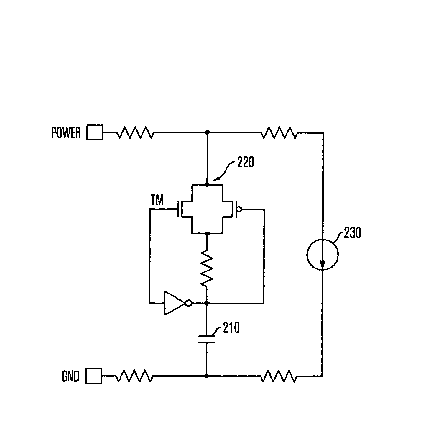
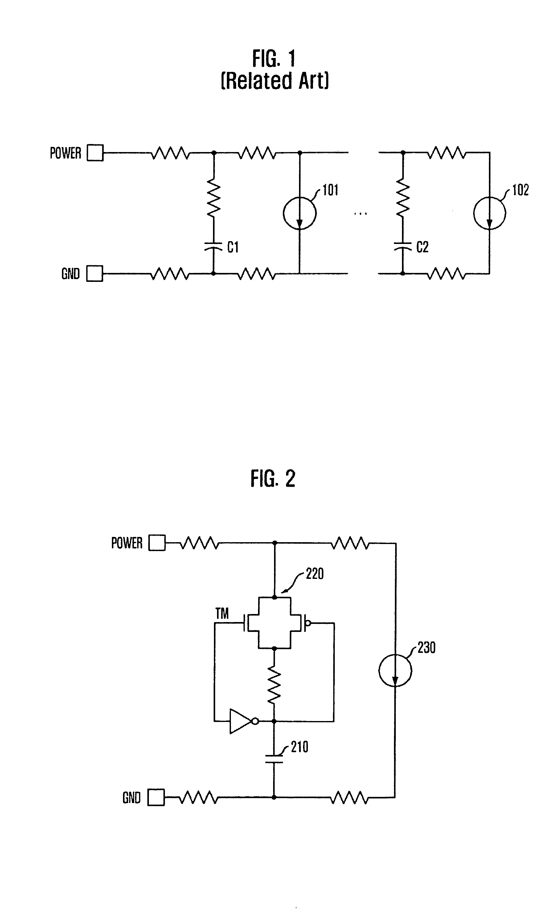
[0021]FIG. 2 is a circuit diagram of a semiconductor device in accordance with an embodiment of the invention.

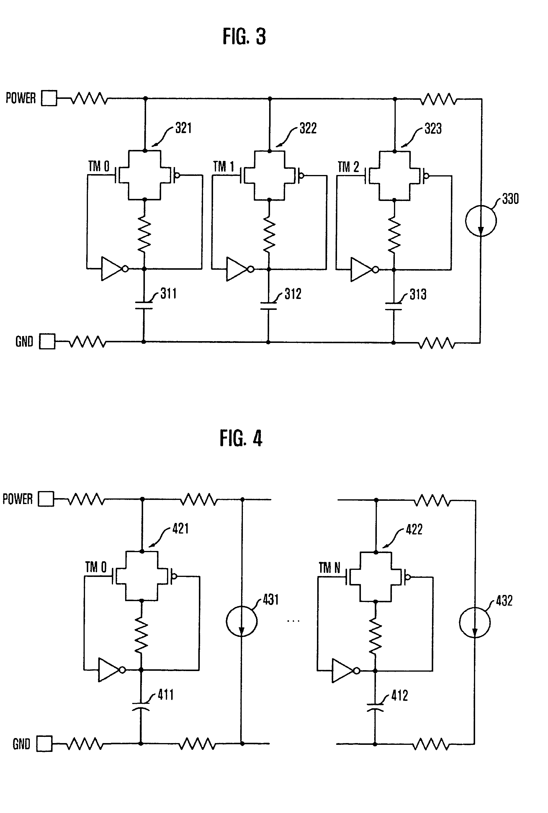
[0022]Referring to FIG. 2, the semiconductor device includes a decoupling capacitor 210 connected between a power voltage terminal POWER and a ground terminal GND. The device also includes a switching unit 220 enabling / disabling the decoupling capacitor 210 in response to a control signal TM. A current source 230 represents circuits inside a chip consuming a current, i.e. 230 represents a load.

[0023]The decoupling capacitor 210 is connected between the power voltage te...


PUM


Abstract

Semiconductor device with a controllable decoupling capacitor includes a decoupling capacitor connected between a power voltage terminal and a ground terminal and a switching unit configured to enable/disable the decoupling capacitor in response to a control signal. According to another aspect, a semiconductor device with a controllable decoupling capacitor includes multiple circuits, decoupling capacitors being connected in parallel to each of the circuits and switching units being configured to enable/disable the decoupling capacitors in response to control signals.

Description

CROSS-REFERENCE TO RELATED APPLICATIONS[0001]The present invention claims priority of Korean patent application number 10-2007-0111348, filed on Nov. 2, 2007, which is incorporated by reference in its entirety.BACKGROUND OF THE INVENTION[0002]The present invention relates to a decoupling capacitor suppressing a high frequency noise in a semiconductor device, and more particularly, to technology for improving screening ability while a semiconductor device is tested through control of a decoupling capacitor.[0003]In a semiconductor device, a decoupling capacitor is a capacitor used for removing an on-chip high frequency noise. Particularly, the decoupling capacitor prevents a portion of the semiconductor device that supplies a voltage from being influenced by a noise caused by an internal / external condition.[0004]Most of semiconductor devices include lots of circuits generating a voltage from the inside of the semiconductor besides a voltage supplied from the outside. For example, a s...

Claims


Application Information

Patent Timeline
IPC IPC(8): G05F1/46
CPCH01L23/5223H03H1/00H03H2001/0064H01L2924/0002H01L2924/00G11C7/00
Inventor LEE, HYUNG-DONGLEE, JUN-HOKIM, DONG-HWEEYANG, HWA-YONG
Owner SK HYNIX INC
Why Eureka
Try Eureka