Bidirectional shift register and display device using the same

a technology of bidirectional shift and register, applied in the direction of digital storage, static storage, instruments, etc., can solve the problem of large circuit siz

Active Publication Date: 2009-05-07
NEC LCD TECH CORP
View PDF7 Cites 32 Cited by
  • Summary
  • Abstract
  • Description
  • Claims
  • Application Information

AI Technical Summary

Benefits of technology

[0025]The shift register in which the shift register stages 212 are connected in series in this way does not require signals (P and N in FIG. 29) prescribing scanning direction, with regard to Patent Document 1, and realizes bidirectional scanning.

Problems solved by technology

Realizing a liquid crystal display device with high added value, using a conventional bidirectional shift register, has the following problems.
Accordingly, since the bidirectional shift register with such a configuration needs to have circuit elements that are active and inactive according to scanning direction, there is a tendency for circuit size to become large.

Method used


Image

  • Bidirectional shift register and display device using the same
  • Bidirectional shift register and display device using the same
  • Bidirectional shift register and display device using the same

Examples


first exemplary embodiment

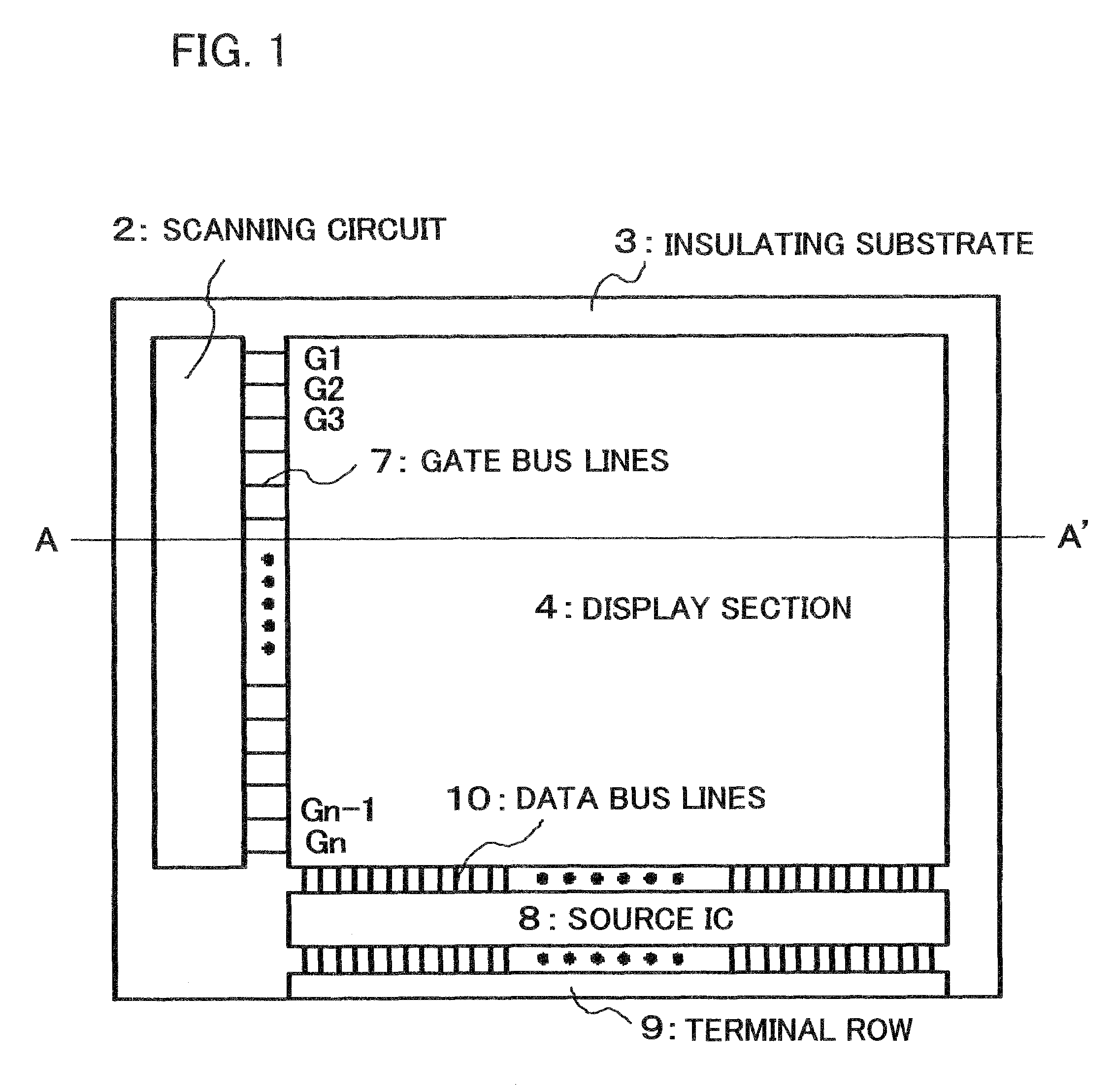
[0104]FIG. 1 is a drawing showing a configuration of a display device according to a first exemplary embodiment of the present invention. In FIG. 1, in the display device, a display section 4, a scanning circuit 2, gate bus lines 7 (G1, G2, G3, . . . Gn−1, Gn), a source IC 8, a terminal row 9, and data bus lines 10 are installed on an insulating substrate 3, formed from transparent glass substrate. The scanning circuit 2 drives gates of switch transistors of pixels in the display section 4, via the gate bus lines 7. Furthermore, the source IC 8 supplies signals inputted from the terminal row 9 to sources of the switch transistors of the pixels of the display section 4, via the data bus lines 10. In the display section 4, a plurality of pixels, as shown in FIG. 6, described later, is arrayed.

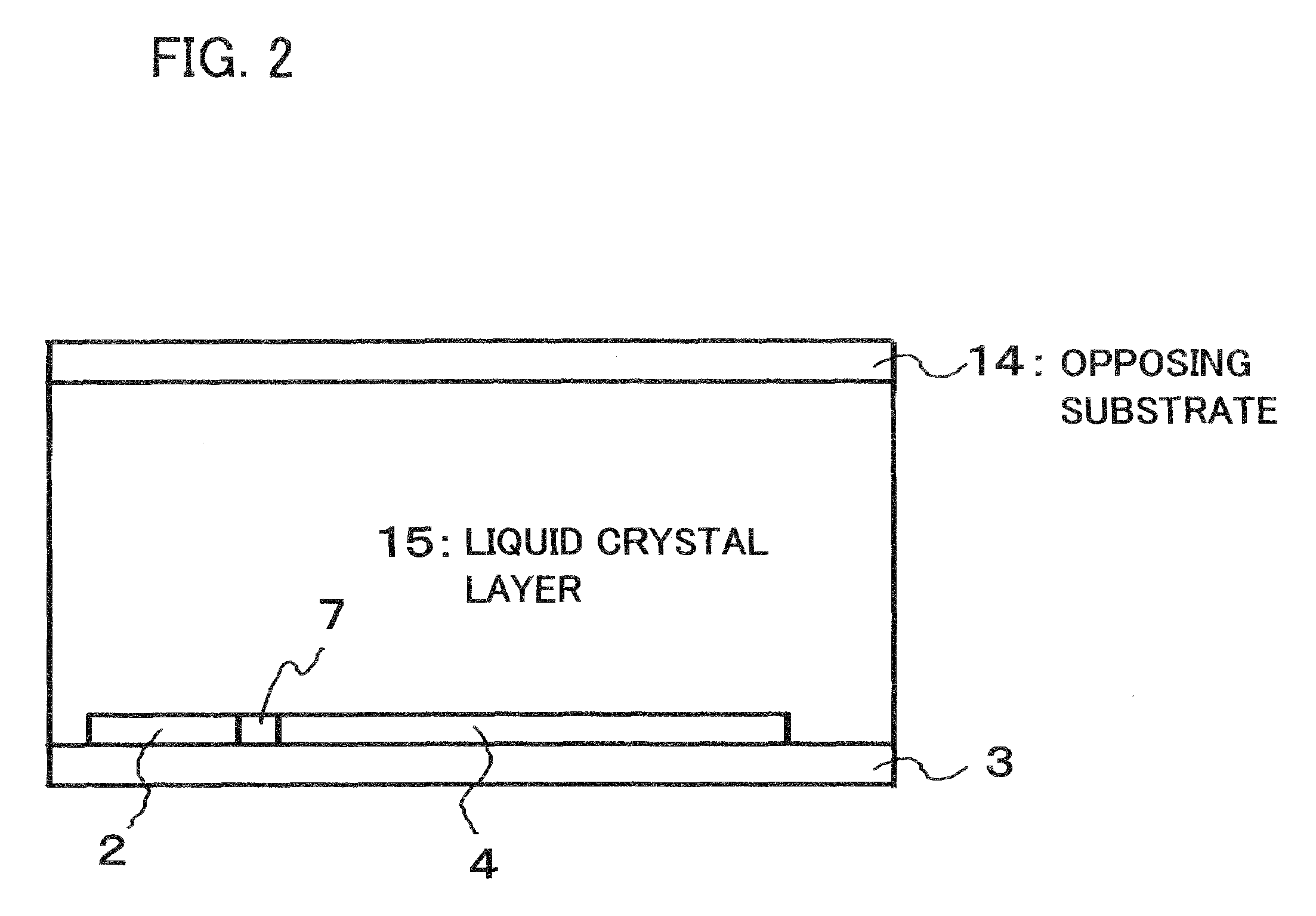
[0105]FIG. 2 is a cross-sectional view (A-A′) of FIG. 1. In FIG. 2, the display device is composed of the insulating substrate 3, an opposing substrate 14, and a liquid crystal layer 15, and the ...

second exemplary embodiment

[0142]A display device according to a second exemplary embodiment of the present invention, as shown in FIG. 9 and FIG. 10, is similar to configurations shown in FIG. 1 and FIG. 2. However, switch transistors in pixels composing the display section 4 are PMOS transistors 13a as shown in FIG., 11. Furthermore, as shown in FIG. 9, all transistors Tr1a˜Tr11a composing the shift register 1 of FIG. 4 in the first exemplary embodiment and all transistors Tr20a˜Tr25a composing the switch array 30a of FIG. 10 are PMOS transistors. In addition, VDD is connected instead of VSS. Connection configuration is similar to the first exemplary embodiment.

[0143]The shift register(s) and switch array configured as above operate similarly to those described in the first exemplary embodiment. However, levels of all signals shown in FIG. 12 and FIG. 13 are the inverse of levels of signals shown in FIG. 7 and FIG. 8, respectively.

[0144]As described above, in cases in which PMOS transistors are used as in t...

third exemplary embodiment

[0145]The display device according to a third exemplary embodiment of the present invention is similar to configurations shown in FIG. 1 and FIG. 2. Furthermore, similar circuits are applied to the shift registers of the first exemplary embodiment shown in FIG. 4 and the pixel portion shown in FIG. 6. In the present exemplary embodiment, the fact that a scanning circuit operates by four phase clock signals (CLK1, CLK2, CLK3, CLK4) is different from the first exemplary embodiment.

[0146]FIG. 14 is a drawing showing a configuration of a scanning circuit according to the third exemplary embodiment of the present invention. In FIG. 14, the scanning circuit 2b is composed of a plurality of shift registers 1 (unit registers represented by SR1, SR2, . . . SRn), a plurality of switch arrays 30b (SA1, . . . SAm), and line groups (lines connected to terminals CLK1, CLK2, CLK3, CLK4, ST1, ST2, FW, and RV). Gate bus lines 7 are connected to OUT terminals of each of the shift registers 1 of the s...


PUM


Abstract

A device, in which circuit size is small and operation is stable, comprises a plurality of serially connected unit registers (shift registers) in which transfer is controlled by any of three or more clock signals each having a different phase, and a setting signal which determines shift direction; and a selection circuit (switch array) which can select at least one clock signal from the three or more clock signals in accordance with the setting signal; wherein the unit registers are put in a reset state by one clock signal selected by the selection circuit, corresponding to each of the unit registers

Description

REFERENCE TO RELATED APPLICATION[0001]This application is based upon and claims the benefit of the priority of Japanese patent applications No. 2007-288754 filed on Nov. 6, 2007, and No. 2008-083673 filed on Mar. 27, 2008, the disclosure of which is incorporated herein in its entirety by reference thereto.FIELD OF THE INVENTION[0002]This invention relates to bidirectional shift registers and to display devices using the same, and in particular, to a bidirectional shift register preferably used in a scanning circuit, and to a display device using the same.BACKGROUND OF THE INVENTION[0003]Since flat display devices represented by liquid crystal display devices, are thin, light-weight, and have low power consumption, they are widely used as display devices in all types of apparatus. Recently, in order to realize even thinner, lighter and lower cost devices, in comparison with conventional amorphous silicon thin film transistors, technology has been established in which a drive circuit ...

Claims


Application Information

Patent Timeline
Patent Type & Authority Applications(United States)
IPC IPC(8): G09G5/36G11C19/28G11C19/00
CPCG11C19/28G09G3/3677
Inventor OTOSE, TOMOHIKOSHIMODA, MASAMICHI
Owner NEC LCD TECH CORP
Why Eureka
Try Eureka