

Semiconductor memory device and method of operating the same
a semiconductor memory and memory device technology, applied in the direction of digital storage, instruments, and increasing the degree of modification, can solve the problems of delay amount, insufficient operation margin of 14 period of system clock, and inability to meet the required synchronous semiconductor memory device, etc., and achieve the effect of constant operation margin
- Summary
- Abstract
- Description
- Claims
- Application Information
AI Technical Summary
Benefits of technology
Problems solved by technology
Method used
Image

Examples
Embodiment Construction
[0039]Hereinafter, a semiconductor memory device in accordance with the present invention will be described in detail with reference to the accompanying drawings.
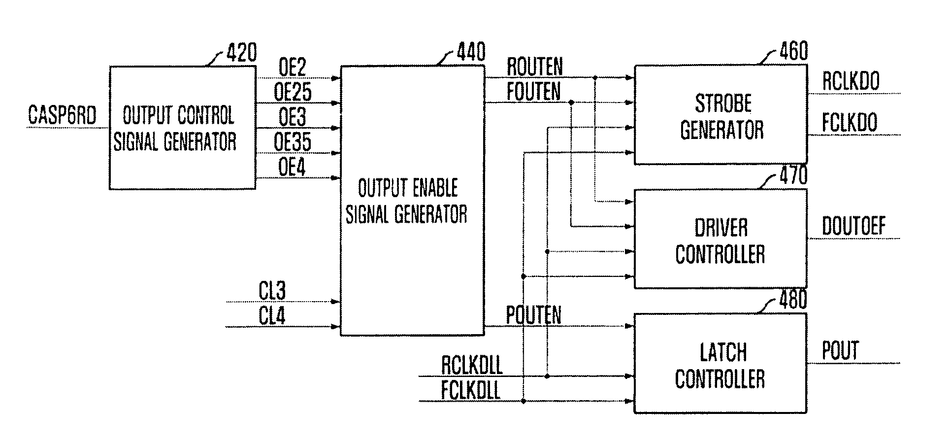
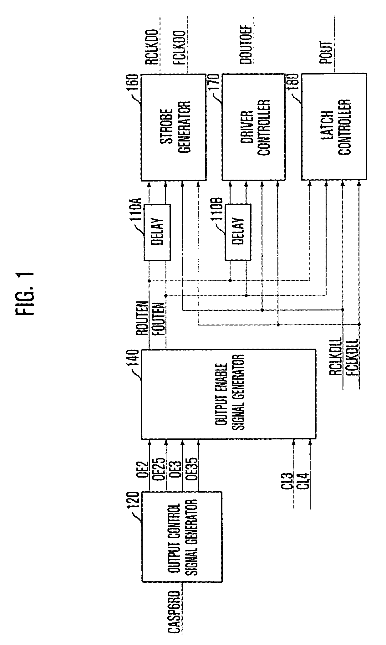
[0040]The semiconductor memory device of the invention may include a data output control circuit configured to control data outputted in synchronization with a falling edge of a system clock using a first output source signal synchronized with a rising edge of the system clock, and to control data outputted in synchronization with the rising edge of the system clock using a second output source signal synchronized with a falling edge of the system clock, and a data output circuit (not shown) configured to output data received from the inside to the outside, the data output circuit being controlled by the data output control circuit. Herein, data output circuit may include a pipeline latch configured to temporarily store data for aligning the data outputted from a plurality of unit cells, and an output driver configured to o...
PUM
 Abstract
Description
Claims
Application Information