Semiconductor integrated circuit device

Inactive Publication Date: 2005-01-06
HITACHI LTD
View PDF2 Cites 28 Cited by
  • Summary
  • Abstract
  • Description
  • Claims
  • Application Information

AI Technical Summary

Benefits of technology

[0012] This invention provides ways for maintaining operation margin and realizing low power consumpti

Problems solved by technology

Therefore, a problem arises in a bit line (or data line) connecting a plurality of static type memory cells which comprise a MOSFET with a low threshold voltage, that is, the ope

Method used


Image

  • Semiconductor integrated circuit device
  • Semiconductor integrated circuit device
  • Semiconductor integrated circuit device

Examples


Embodiment Construction

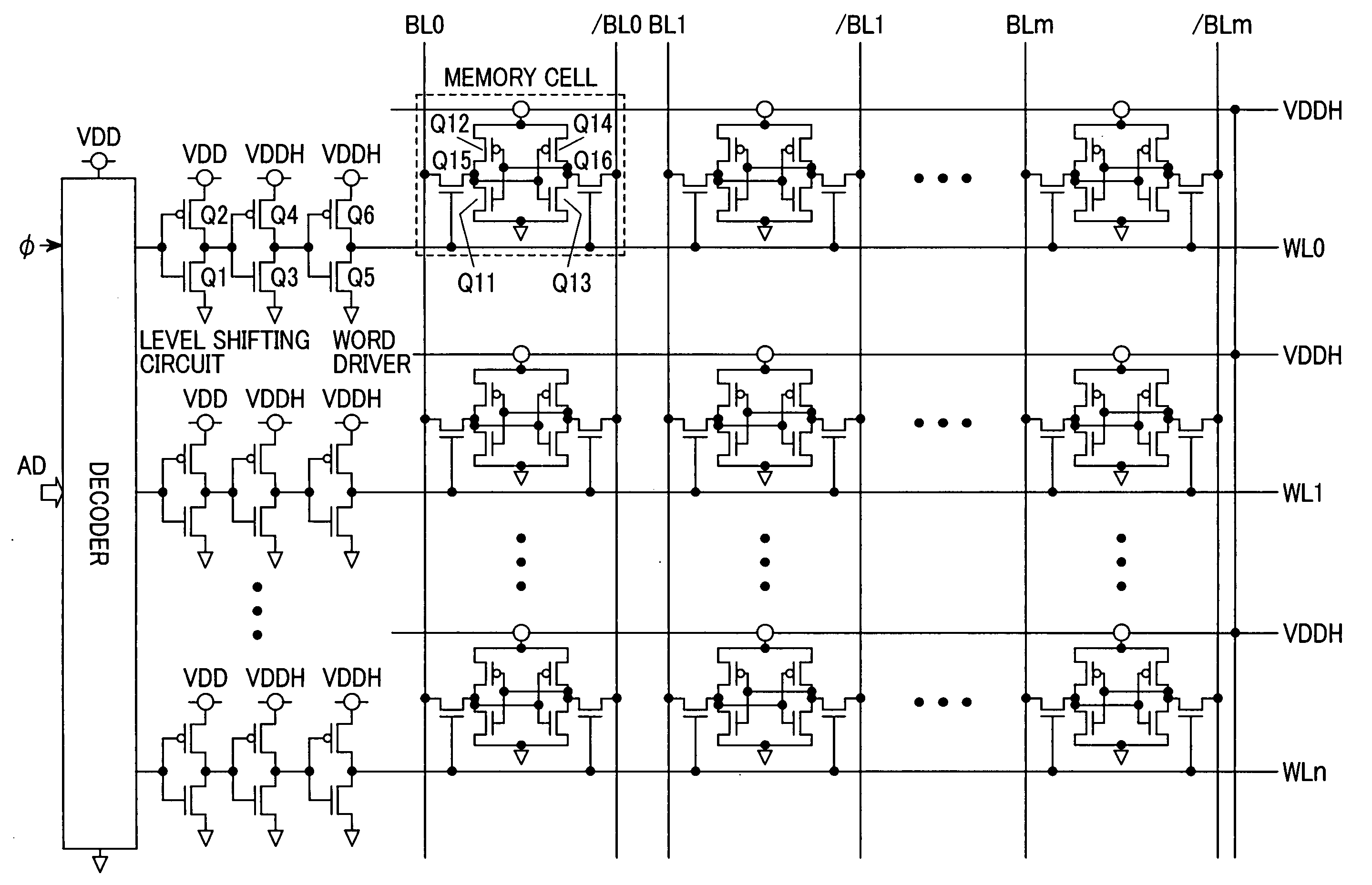
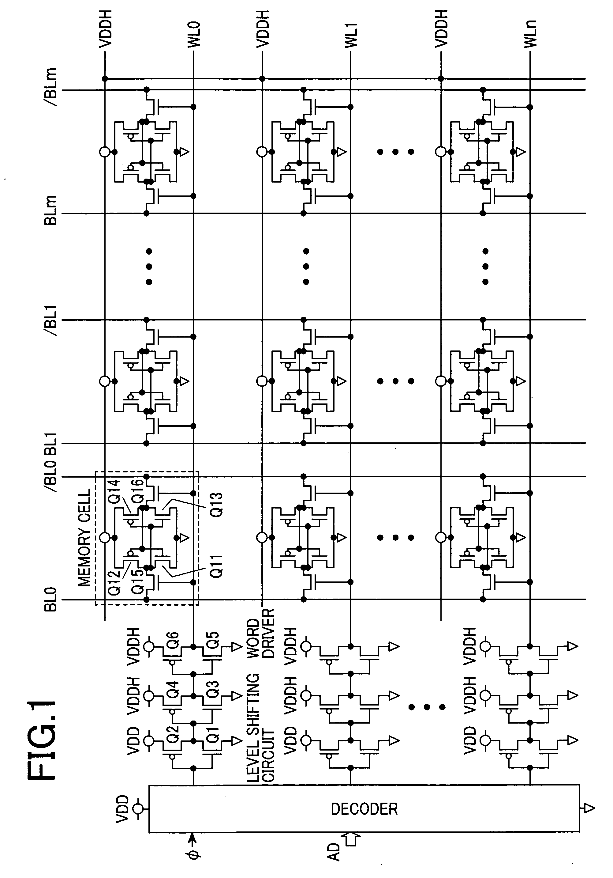
[0019]FIG. 1 shows a schematic circuit diagram by a way of example of a memory circuit mounted in a semiconductor circuit device related to this invention. In the figure, a memory cell array comprising a memory circuit and a word driver working for selection of the word line are illustrated by way of example. The memory array comprises a plurality of memory cells installed at the cross point of complementary bit lines of BLO / BLO or BLm / BLm and word lines WLO or WLn.

[0020] As the memory cell, a CMOS latch circuit composed of the intersecting connection of outputs and inputs of two CMOS inverter circuits which consist of N-channel MOSFETQ11, Q13 and P-channel MOSFETQ12, Q14 is used, and CMOS static type memory cell comprised of N-channel MOSFETQ15, Q16 installed between the pair of input / output nodes and the bit line is also used. The gates of said MOSFETQ15 and Q16 are connected with word line WLO etc. corresponding to them. One source and drain of said MOSFETQ15, Q16 are connected ...


PUM


Abstract

A semiconductor integrated circuit device endowed with memory circuits achieving high operation margin and low energy consumption with high speed and high integration. Composing a memory cell with a MOSFET having a first threshold voltage corresponding to a first voltage and supplying a selection signal corresponding to said first voltage to a word line by a word driver driven at said first voltage. Corresponding to a second voltage smaller than said first voltage, forming a selection signal sending to said word driver by a decoder comprising MOSFET with a second threshold voltage smaller than said first voltage, operating at said first voltage, and installing a first level shifting circuit including inverter circuits that form a selection signal corresponding to said first voltage by receiving a selection signal corresponding to said second voltage. Thereby, high operation margin and low energy consumption with high speed and high integration can be achieved.

Description

CLAIM OF PRIORITY [0001] The present application claims priority from Japanese application JP 2003-270807 field on Jul. 3, 2003, the content of which is hereby into this application. FIELD OF THE INVENTION [0002] This invention relates to a semiconductor integrated circuit and relates to an effective method applied to a semiconductor integrated circuit consisting, for instance, of miniaturized elements and comprising a logical circuit and a memory circuit. BACKGROUND OF THE INVENTION [0003] According to a well-known example investigation after this invention had been done, the following patent document 1 was reported as one relating to this invention. In this patent document 1, a memory comprising two power supplies, which supply a higher voltage to a memory cell than the surrounding, is disclosed. In this patent document 1, an applied voltage to a power supply line of a memory cell or a word line is stepped-up, and the conception is different from this invention described later. [0...

Claims


Application Information

Patent Timeline
IPC IPC(8): G11C11/417G11C7/00G11C8/00G11C8/08G11C11/413G11C11/418H01L21/8234H01L21/8244H01L27/088H01L27/10H01L27/11H03K5/153H03K19/0185
CPCG11C8/08H03K19/018521G11C11/418G11C11/413
Inventor KAWATA, TAKAHIRONAKAHARA, SHIGERUHIGETA, KEIICHI
Owner HITACHI LTD
Why Eureka
Try Eureka