Wafer lens aligning method and wafer lens manufactured by the same

Inactive Publication Date: 2009-06-25
SAMSUNG ELECTRO MECHANICS CO LTD
View PDF5 Cites 13 Cited by
  • Summary
  • Abstract
  • Description
  • Claims
  • Application Information

AI Technical Summary

Benefits of technology

[0020]An advantage of the present invention is that it provides a wafer lens aligning method, in which the coordinate system of a wafer is set by position recognition patterns formed at arbitrary positions, a mold is moved in accordance with the set coordinate system, and minute patterns formed in each lens formation position of the wafer are aligned with a groove formed on the mold such that the mold can be accurately aligned with the lens formation position.
[0021]Another advantage of the invention is that it provides a wafer lens manufactured by the wafer lens aligning method.
[0022]Additional aspects and advantages of the present general inventive concept will be set forth in part in the description which follows and, in part, will be obvious from the description, or may be learned by practice of the general inventive concept.
[0023]According to an aspect of the invention, a wafer lens aligning method comprises the steps of: preparing a lens mold that has a lens forming portion formed in the central portio

Problems solved by technology

In such an aligning method, however, the outer circumferential surface of the mold is not relatively precisely processed, compared with a lens forming portion which is precisely processed.
However, when the mold is attached to and detached from a jig connected to the motor, an assembling error may occur.
Further, the mold is

Method used


Image

  • Wafer lens aligning method and wafer lens manufactured by the same
  • Wafer lens aligning method and wafer lens manufactured by the same
  • Wafer lens aligning method and wafer lens manufactured by the same

Examples


Example

[0040]Reference will now be made in detail to the embodiments of the present general inventive concept, examples of which are illustrated in the accompanying drawings, wherein like reference numerals refer to like elements throughout. The embodiments are described below in order to explain the present general inventive concept by referring to the figures.

[0041]Hereinafter, a wafer lens aligning method and a wafer lens manufactured by the same according to an embodiment of the present invention will be described in detail with reference to the accompanying drawings.

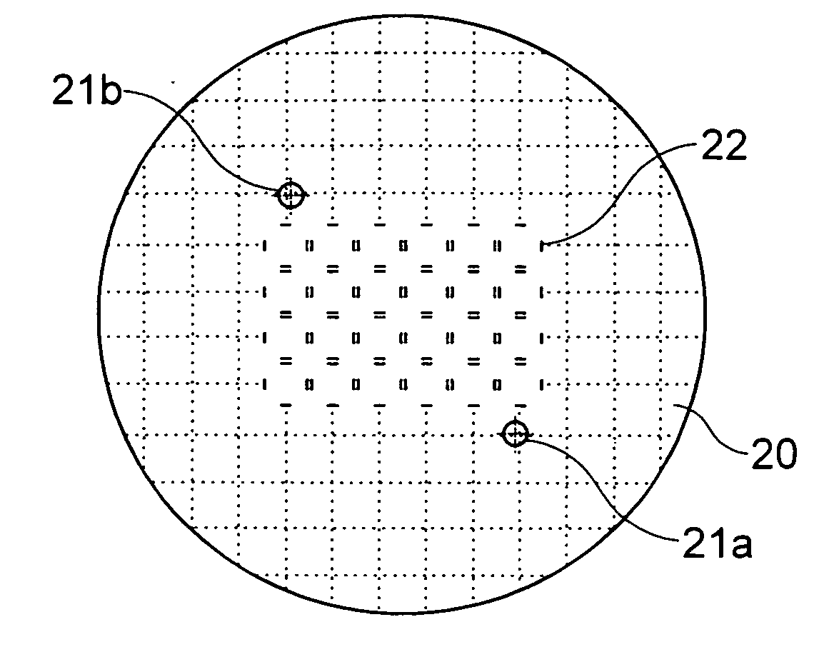
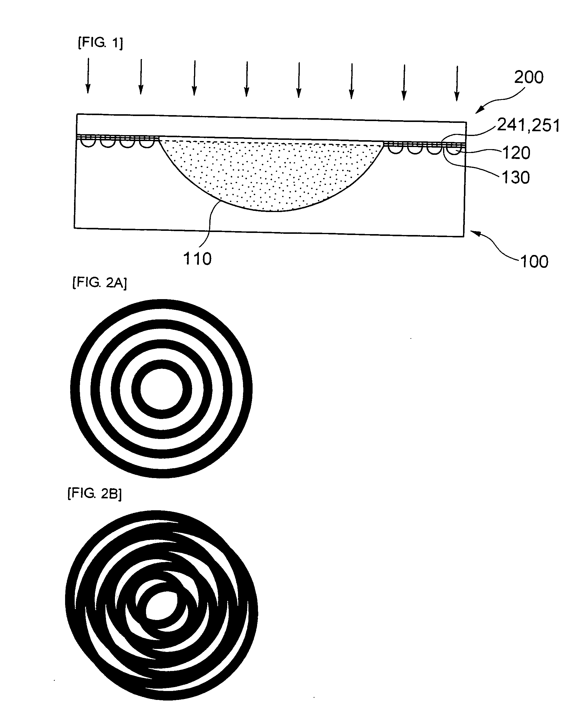
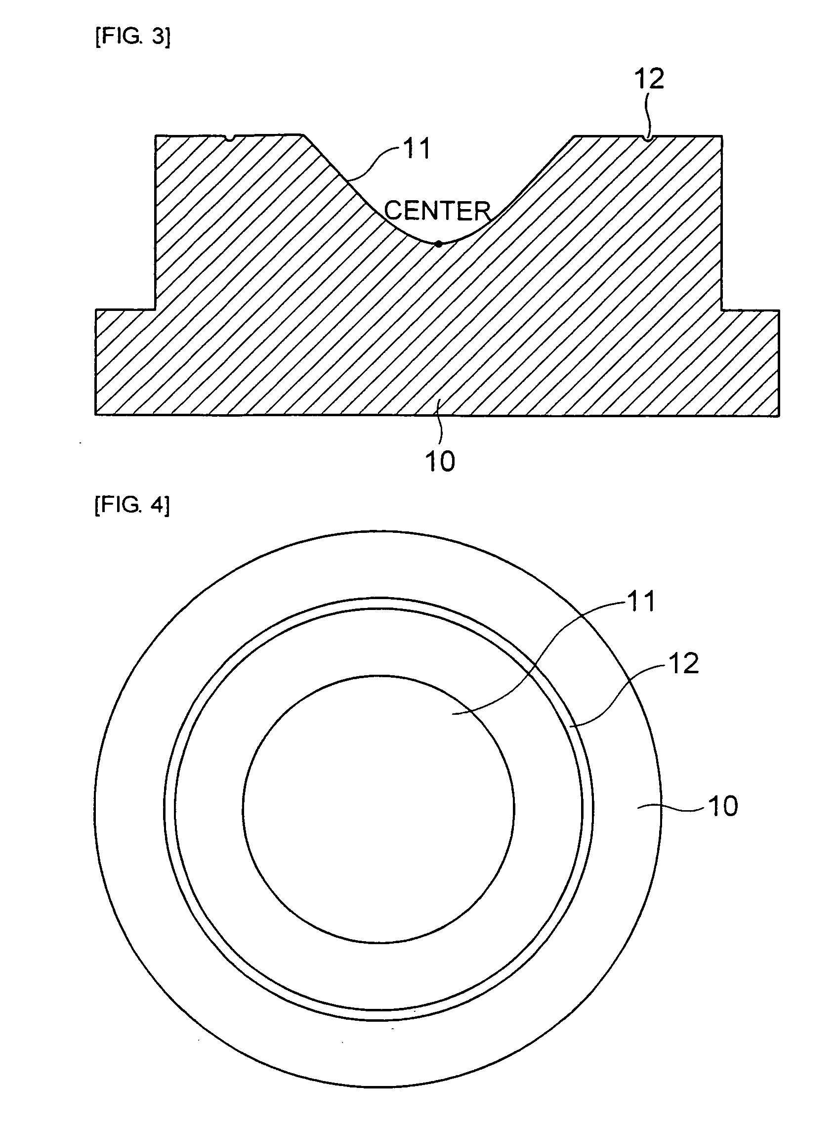
[0042]FIG. 3 is a cross-sectional view of a mold which is adopted in a wafer lens aligning method according to the invention. FIG. 4 is a plan view of the mold of FIG. 3.

[0043]As shown in the drawings, the lens mold 100 adopted in the wafer lens aligning method according to the invention has a lens forming portion 11, into which polymer-based resin is injected to mold a lens and which is formed in the central portion there...


PUM


Abstract

Provided is a wafer lens aligning method including the steps of: preparing a lens mold that has a lens forming portion formed in the central portion thereof and a groove formed around the lens forming portion; preparing a wafer that has two or more position recognition patterns formed at arbitrary positions thereof and a plurality of minute patterns formed in array at lens formation positions; loading the wafer, searching the position recognition patterns, and setting a coordinate system; causing the coordinate system of the wafer to coincide with the coordinate system of the lens mold; causing the center among the minute patterns formed on the wafer to coincide with the center of the lens mold so as to align the wafer with the lens mold; and forming a master lens in the lens formation positions arranged on the wafer.

Description

CROSS-REFERENCE TO RELATED APPLICATIONS[0001]This application claims the benefit of Korean Patent Application No. 10-2007-0134231 filed with the Korea Intellectual Property Office on Dec. 20, 2007, the disclosure of which is incorporated herein by reference.BACKGROUND OF THE INVENTION[0002]1. Field of the Invention[0003]The present invention relates to a wafer lens aligning method and a wafer lens manufactured by the same.[0004]2. Description of the Related Art[0005]In general, a mastering process, a stamping process, an embossing process, and a dicing process are sequentially performed to manufacture a plurality of wafer lenses in the form of single lens.[0006]In this case, polymer which is to be cured by ultraviolet (UV) light is injected into a mold for molding a lens in the mastering process. Further, the polymer is attached on one surface of a substrate-type wafer and is cured by UV irradiation such that a lens is attached to the surface of the wafer. Then, the lens is transfer...

Claims


Application Information

Patent Timeline
IPC IPC(8): G01B11/00
CPCB29D11/005B29D11/00365G02B3/0075G02B7/003G02B13/0085G02B27/1073
Inventor SHIN, DONG IKKIM, HYUN JUNLEE, SEOK CHEONKIM, SUN OK
Owner SAMSUNG ELECTRO MECHANICS CO LTD
Why Eureka
Try Eureka