

Compact Inductive Power Electronics Package
a technology of inductive power and electronics, applied in the direction of magnets, cores/yokes, magnets, etc., can solve the problems of frame inductor being unable to meet power applications, fragile ferrite chip exposed without protection, etc., to save package foot prints and
- Summary
- Abstract
- Description
- Claims
- Application Information
AI Technical Summary
Benefits of technology
Problems solved by technology
Method used
Image

Examples
sixth embodiment
[0051]Fig. D1 is a top plan view of another embodiment of a semiconductor power device package having a lead frame-based integrated inductor in accordance with the invention. Fig. D2 is a top plan view of a bottom portion of a semiconductor power device package having a lead frame-based integrated inductor in accordance with the invention.
[0052]An embodiment of the invention is shown in Fig. D1 and includes a semiconductor power device package 1900 having a lead frame-based integrated inductor 1950. The inductor 1950 is comprised of the ferrite chip 1800, a plurality of adjacent leads of the lead frame 100 and bonding wires 1920e, 1920f, 1920i, 1920j, 1920k and 1920m. Connection chip 500 provides electrical connection by means of vias 510a-510f formed in the connection chip 500. The ferrite chip 1800 is attached to a top surface 150 of the lead frame 100 and is supported by the large pad 120 and the small pad 130. The ferrite chip 1800 is disposed on the top surface 150 of the lead ...
second embodiment
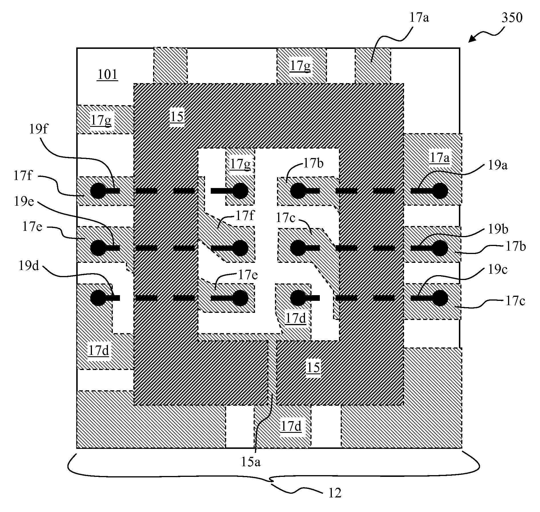
[0063]FIG. 2 illustrates the present invention compact inductive power electronics package 350 with a power inductor 12 of closed magnetic loop located atop a lead frame. The various parts are shown in phantom lines through the encapsulant 101. Like FIG. 1A, the power inductor 12 has a core ferrite chip 15 in the shape of a rectangle with an interior window 16. The lead frame has a first number of bottom half-coil conductive leads 17a through 17g positioned beneath the ferrite chip 15. In essence, the bottom half-coil conductive leads 17a through 17g form a bottom half-coil of the power inductor 12. Correspondingly, a second number of top half-coil forming bond wires 19a through 19f are located atop the ferrite chip 15 with each bond wire looping the ferrite chip 15 from above. Furthermore, both ends of each top half-coil forming bond wire are connected to proper alternative bottom half-coil conductive leads so as to jointly form an inductive coil enclosing the ferrite chip 15. Thus...
PUM
| Property | Measurement | Unit |
|---|---|---|
| Electrical inductance | aaaaa | aaaaa |
| Shape | aaaaa | aaaaa |
| Electrical conductor | aaaaa | aaaaa |
Abstract
Description
Claims
Application Information