

Liquid Crystal Display Panel and Liquid Crystal Display
a liquid crystal display panel and liquid crystal display technology, applied in non-linear optics, instruments, optics, etc., can solve the problems of non-uniform illumination, inability to control the thickness of the liquid crystal layer, and more difficult to make all the spacers return to their original position, so as to reduce the defect of image display
- Summary
- Abstract
- Description
- Claims
- Application Information
AI Technical Summary
Benefits of technology
Problems solved by technology
Method used
Image

Examples
first embodiment
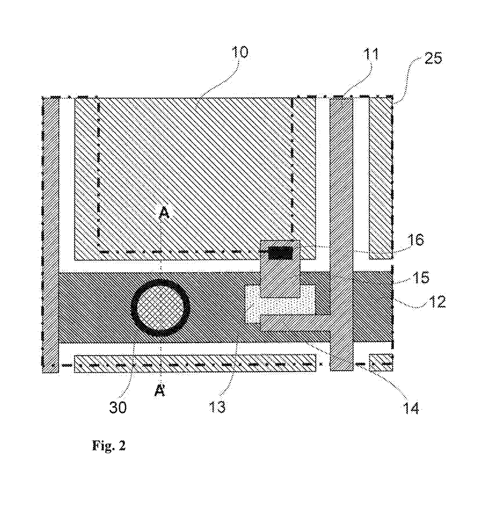
[0042]FIG. 4 is a planar schematic diagram of a liquid crystal display panel according to the present invention. FIG. 4a is a cross-sectional diagram of a first spacer of FIG. 4 taken along line O-O′. FIG. 4b is a cross-sectional diagram of a second spacer of FIG. 4 taken along line F-F′. FIG. 4c is a cross-sectional diagram of a third spacer of FIG. 4 taken along line H-H′. The schematic diagrams are illustrative and can not limit the protection scope of the present invention.
[0043]In the liquid crystal display panel according to the first embodiment of the present invention, as illustrated in FIG. 4, the liquid crystal display panel includes an upper transparent substrate and a lower transparent substrate opposite to and insulated from the upper transparent substrate. A black matrix is configured in a surface of the upper substrate opposite to the lower substrate. The dash line block 25 of FIG. 4 shows the position of the black matrix of the upper substrate. The black matrix corre...
second embodiment
[0052]FIG. 5 is a planar schematic diagram of a liquid crystal display panel according to the present invention. FIG. 5a is a cross-sectional diagram of a first spacer of FIG. 5 taken along line M-M′. FIG. 5b is a cross-sectional diagram of a second spacer of FIG. 5 taken along line L-L′. FIG. 5c is a cross-sectional diagram of a third spacer of FIG. 5 taken along line N-N′. The schematic diagrams are illustrative and can not limit the protection scope of the present invention.
[0053]The liquid crystal display panel according to the second embodiment of the present invention as shown in FIG. 5 is the same as that in FIG. 4 except that spacers are different, so that the repeated explanations for the same structure between FIG. 5 and FIG. 4 will be omitted. The spacers in FIG. 5 include the first spacer 30 at line M-M′, the second spacer 30′ at line L-L′ and the third spacer 30″ at line N-N′, as illustrated in FIGS. 5a, 5b and 5c, respectively. Further, the distribution density of the ...
third embodiment
[0058]FIG. 6 is a planar diagram of a liquid crystal display panel according to the present invention. FIG. 6a is a cross-sectional diagram of a first spacer of FIG. 6 taken along line J-J′. FIG. 6b is a cross-sectional diagram of a second spacer of FIG. 6 taken along line I-I′. FIG. 6c is a cross-sectional diagram of a third spacer of FIG. 6 taken along line K-K′. The schematic diagrams are illustrative and can not limit the protection scope of the present invention.
[0059]The liquid crystal display panel according to the third embodiment of the present invention as shown in FIG. 6 is the same as that in FIG. 4 except for the spacers, so that the repeated explanations for the same structure will be omitted. The spacers in FIG. 6 includes the first spacer 30 at line J-J′, the second spacer 30′ at line I-I′, the third spacer 30″ at line K-K as illustrated in FIGS. 6a, 6b and 6c, respectively. Further, the distribution density of the first spacers 30 is larger than that of the second s...
PUM
 Abstract
Description
Claims
Application Information