Control of implant critical dimensions using an sti step height based dose offset

a technology of critical dimensions and ion implants, applied in the field of semiconductor processing, can solve the problems of device performance, device isolation parametrics, device performance, and production yield, and achieve the effect of improving cd control in semiconductor processing and improving the critical dimension of ion implants

Active Publication Date: 2009-07-02
TEXAS INSTR INC
View PDF6 Cites 4 Cited by
  • Summary
  • Abstract
  • Description
  • Claims
  • Application Information

AI Technical Summary

Benefits of technology

[0009]The present invention addresses the need for improved CD control in semiconductor processing, especially in regards to ion implantation processes. The following presents a simplified summary of the invention in order to provide a basic understanding of some aspects of the invention. This summary is not an extensive overview of the invention. It is intended to neither identify key or critical elements of the invention nor delineate the scope of the invention. Its purpose is to present some concepts of the invention in a simplified form as a prelude to the more detailed description that is presented later.
[0010]The present invention is generally directed toward a method for semiconductor processing. The method comprises providing a semiconductor wafer that underwent polishing. The semiconductor wafer comprises an active region positioned between one or more moat regions. The one or more moat regions comprise an oxide. A top surface of the active region is recessed from a top surface of the moat region. A step is defined by a step height. The step height is determined. A photoresist is formed over the semiconductor wafer. The method further comprises determining a modeled step height. The modeled step

Problems solved by technology

The oxide, however, not only fills the trenches, but also creates a layer of oxide over the entire surface of the wafer.
However, variations in implant CDs can have deleterious results on device isolation parametrics, device performance, and production yiel

Method used


Image

  • Control of implant critical dimensions using an sti step height based dose offset
  • Control of implant critical dimensions using an sti step height based dose offset
  • Control of implant critical dimensions using an sti step height based dose offset

Examples


Embodiment Construction

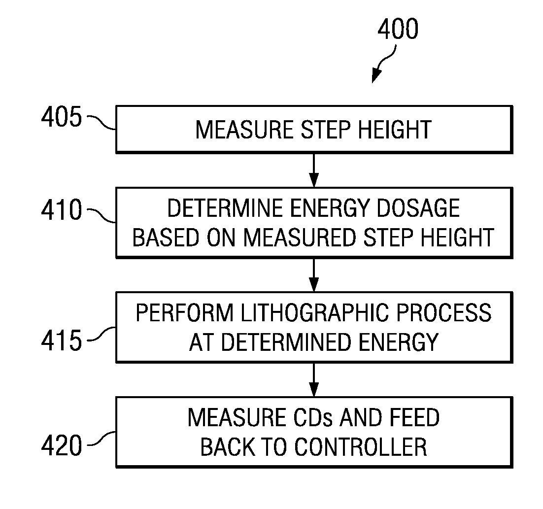
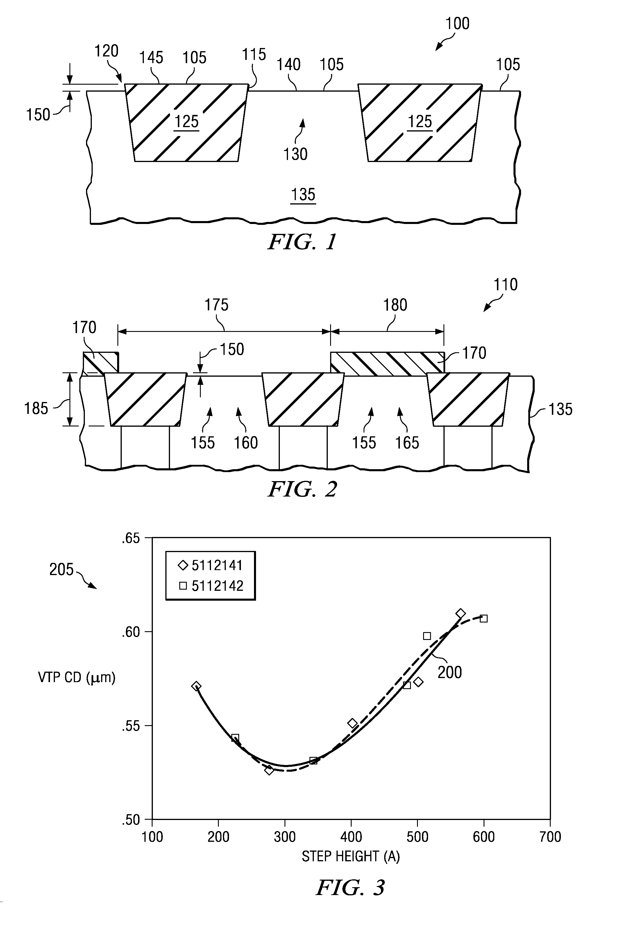
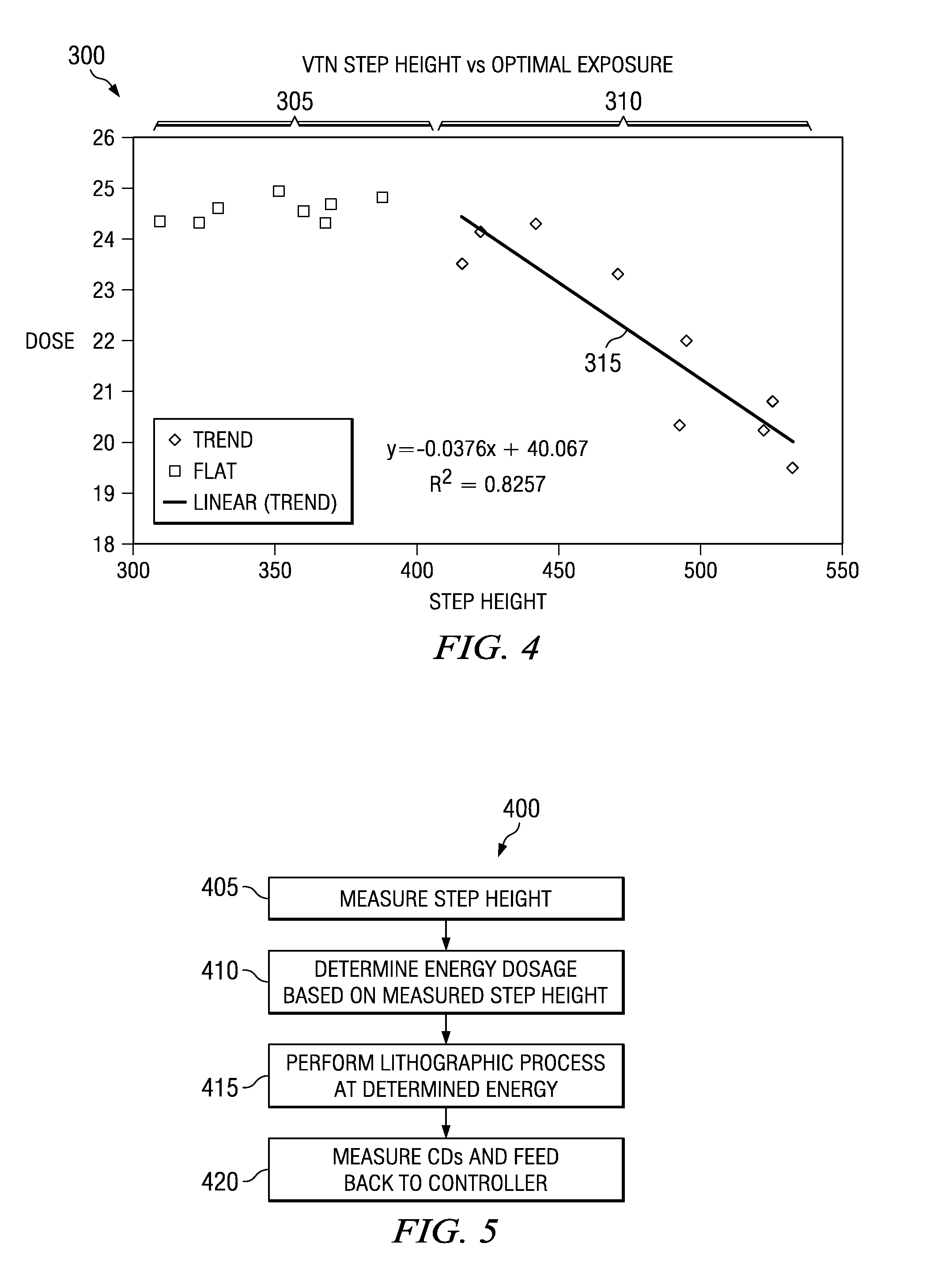
[0017]The present invention is generally directed towards a method for improving critical dimensions during semiconductor processing of a workpiece. In particular, the present invention provides a method for compensating for step heights in shallow trench isolation regions of a workpiece during an ion implantation. Accordingly, the present invention will now be described with reference to the drawings, wherein like reference numerals are used to refer to like elements throughout. It should be understood that the description of these aspects are merely illustrative and that they should not be taken in a limiting sense. In the following description, for purposes of explanation, numerous specific details are set forth in order to provide a thorough understanding of the present invention. It will be evident to one skilled in the art, however, that the present invention may be practiced without these specific details.

[0018]As device sizes in the semiconductor technology continue to decre...


PUM


Abstract

A method for semiconductor processing is provided, wherein a semiconductor wafer having undergone polishing is provided. The semiconductor wafer has an active region positioned between one or more moat regions, wherein the one or more moat regions have an oxide disposed therein. A top surface of the active region is recessed from a top surface of the moat region, therein defining a step having a step height associated therewith. A step height is measured, and a photoresist is formed over the semiconductor wafer. A modeled step height is further determined, wherein the modeled step height is based on the measured step height and a desired critical dimension of the photoresist. A dosage of energy is determined for patterning the photoresist, wherein the determination of the dosage of energy is based, at least in part, on the modeled step height. The photoresist is then patterned using the determined dosage of energy.

Description

REFERENCE TO RELATED APPLICATION[0001]This application claims priority to and the benefit of U.S. Provisional Application Ser. No. 61 / 017,442 which was filed Dec. 28, 2007, entitled “Improved Control of Implant Critical Dimensions Using an STI Step Height Based Dose Offset”, the entirety of which is hereby incorporated by reference as if fully set forth herein.FIELD OF THE INVENTION[0002]The present invention relates generally to semiconductor processing, and more particularly to an improved method for processing STI layers on a substrate.BACKGROUND OF THE INVENTION[0003]Semiconductor processing often involves the formation of components having varying voltage inputs in neighboring regions of a semiconductor wafer.[0004]For example, high-voltage components (e.g., transistors such as DMOS having voltages / currents up to 100V / 2A) are formed in one region of the wafer, while lower-voltage components (e.g., CMOS and flash components) are formed in a neighboring region. In order to provid...

Claims


Application Information

Patent Timeline
IPC IPC(8): H01L21/66
CPCH01L22/20H01L22/12
Inventor REID, BRIAN DOUGLASBERNSTEIN, JAMES DAVIDYUE, HONGYUYANG, HOWIE HUIBOEHM, MARK
Owner TEXAS INSTR INC
Why Eureka
Try Eureka