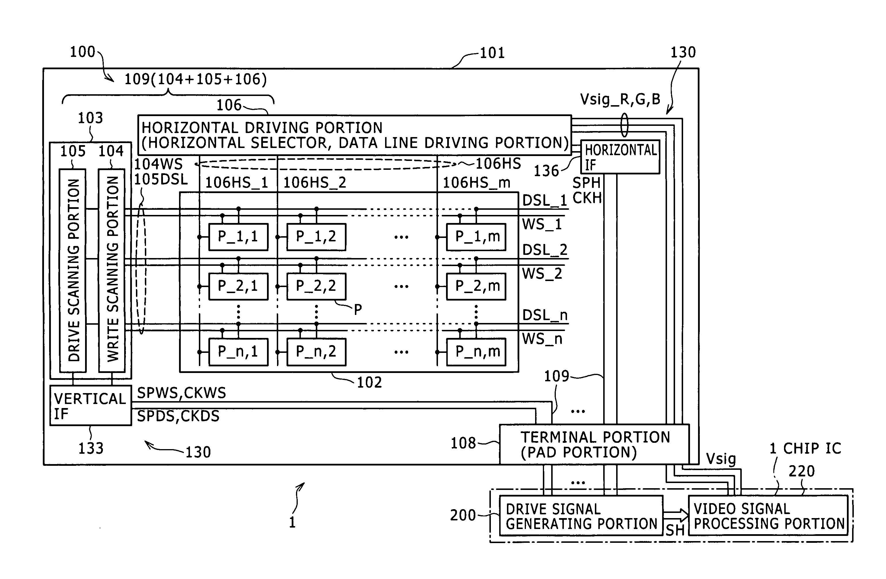
Display Device

Inactive Publication Date: 2009-07-16
SONY CORP
View PDF2 Cites 31 Cited by
  • Summary
  • Abstract
  • Description
  • Claims
  • Application Information

AI Technical Summary

Benefits of technology

[0035]As a result, the timings at which the transistors are driven, respectively, and the like have only to be changed with the 2TR drive configuration as a base. Thus, it is possible to largely reduce the number of constituent elements of the pixel circuit, and the number of wirings, and it is possible to shrink the pixel array portion. As a result, it is easy to carry out the promotion of the high definition for the display device. A part of the scanning line is structured in the form of the subsi

Problems solved by technology

For this reason, there is encountered a problem that, for example, an increase in number of circuit elements, and an increase in capacitance value are not readily carried out, or they become an obstacle to promotion of high definition.
As a result, the configuration of the pixel circuit is complicated.
Many consti

Method used


Image

  • Display Device
  • Display Device
  • Display Device

Examples


first embodiment

Improvement Technique: First Embodiment

[0243]FIGS. 14, 15 and 16 are respectively a diagram, and views explaining a first embodiment of a circuit arrangement (layout) in which an area rate of the scanning lines occupying the TFT layout can be reduced. Here, FIG. 14 shows a basic concept of a layout, of a first embodiment, in the periphery of the pixel circuit P. FIG. 15 is a top plan view of a detailed example (a vertical relationship of the wiring is disregarded) corresponding to FIG. 14. Also, FIG. 16 is a block diagram, partly in cross section, showing a layout of a subsidiary wiring provided in the same layer as that of the lower electrode 504 of the organic EL element 127 corresponding to FIG. 14.

[0244]A point of the improvement technique of this embodiment, including a second embodiment which will be described later, features that with regard to the wiring for which especially the small wiring resistance is required, a subsidiary wiring 515 (first subsidiary wiring) is dispose...

second embodiment

Improvement Technique: Second Embodiment

[0253]FIGS. 17 to 20 are respectively a diagram, and views explaining a second embodiment of a circuit arrangement (layout) in which an area rate of the scanning lines occupying the TFT layout can be reduced. Here, FIG. 17 is a circuit diagram, partly in block, showing a basic concept of a layout of the second embodiment in the periphery of the pixel circuit P, FIG. 18 is a top plan view of a detailed example (a vertical relationship of the wirings is disregarded) corresponding to FIG. 17. Also, FIGS. 19 and 20 are respectively block diagrams, partly in cross sections, showing layouts of the subsidiary wirings each provided in the same layer as that of the lower electrode 504 of the organic EL element 127 corresponding to FIG. 17.

[0254]Similarly to the case of the first embodiment, a point of the improvement technique of this embodiment features that with regard to the wiring for which especially the small wiring resistance is required, a subs...


PUM


Abstract

Any one of a write scanning line, a power source supply line, and a video signal line is structured as a subsidiary wiring disposed in the same layer as that having a lower electrode disposed therein. The subsidiary wiring is used in the power source supply line through which a power source drive pulse to be pulse-driven is transmitted, or other wirings (such as the write scanning line and the video signal line).

Description

CROSS REFERENCES TO RELATED APPLICATIONS[0001]The present invention contains subject matter related to Japanese Patent Application JP 2008-006735 filed in the Japan Patent Office on Jan. 16, 2008, the entire contents of which being incorporated herein by reference.BACKGROUND OF THE INVENTION[0002]1. Field of the Invention[0003]The present invention related to a display device including a pixel array portion in which pixel circuits (referred to as “pixels” as well) each having an electro-optic element (referred to as either “a display element” or “a light emitting element” as well) are disposed in a matrix. More particularly, the invention relates to an active matrix type display device in which pixel circuits each having an electro-optic element as a display element having a luminance adapted to change depending on a magnitude of a drive signal are disposed in a matrix, and which includes an active element every pixel circuit, display drive being carried out in units of pixels by th...

Claims


Application Information

Patent Timeline
IPC IPC(8): G09G3/30
CPCG09G3/3233G09G2310/06G09G2300/0426G09G2300/0439G09G2300/0465G09G2300/0819G09G2300/0842G09G2300/0866G09G2310/0256G09G2320/043G09G2320/045G09G3/30G09G3/3225G09G2300/08G09G2310/027G09G3/3266
Inventor YAMASHITA, JUNICHIUCHINO, KATSUHIDE
Owner SONY CORP
Why Eureka
Try Eureka