Soldering Method, Semiconductor Module Manufacturing Method, and Soldering Apparatus

a semiconductor module and manufacturing method technology, applied in the direction of soldering apparatus, manufacturing tools,auxillary welding devices, etc., can solve the problem of damage inflicted on semiconductor elements

Inactive Publication Date: 2009-07-23
TOYOTA IND CORP
View PDF16 Cites 23 Cited by
  • Summary
  • Abstract
  • Description
  • Claims
  • Application Information

AI Technical Summary

Benefits of technology

[0014]Yet another aspect of the present invention is a soldering apparatus for soldering an electronic component onto a circuit board. The soldering apparatus includes a support, a heating medium supply unit and a control unit. The support is capable of supporting the circuit board. The circuit board is a cooling circuit board including an insulation substrate and a metal heat sink. The insulation substrate has a front surface with a metal circuit and a rear surface to which the heat sink is fixed. The heat sink has a refrigerant passage. The refrigerant passage includes an inlet and an outlet. The heating medium supply unit is capable of supplying a heating medium to the refrigerant passage. The heating medium supply unit includes a pipe connectable to the inlet and the outlet in a state in which the cooling circuit board is supported by the support. The control unit controls temperature of the heating medium supplied to the refrigerant passage.

Problems solved by technology

However, if the temperature of the heating body is too high, damages may be inflicted on the semiconductor elements, which are electronic components.

Method used


Image

  • Soldering Method, Semiconductor Module Manufacturing Method, and Soldering Apparatus
  • Soldering Method, Semiconductor Module Manufacturing Method, and Soldering Apparatus
  • Soldering Method, Semiconductor Module Manufacturing Method, and Soldering Apparatus

Examples


first embodiment

[0022]the present invention will now be described with reference to FIGS. 1 to 5.

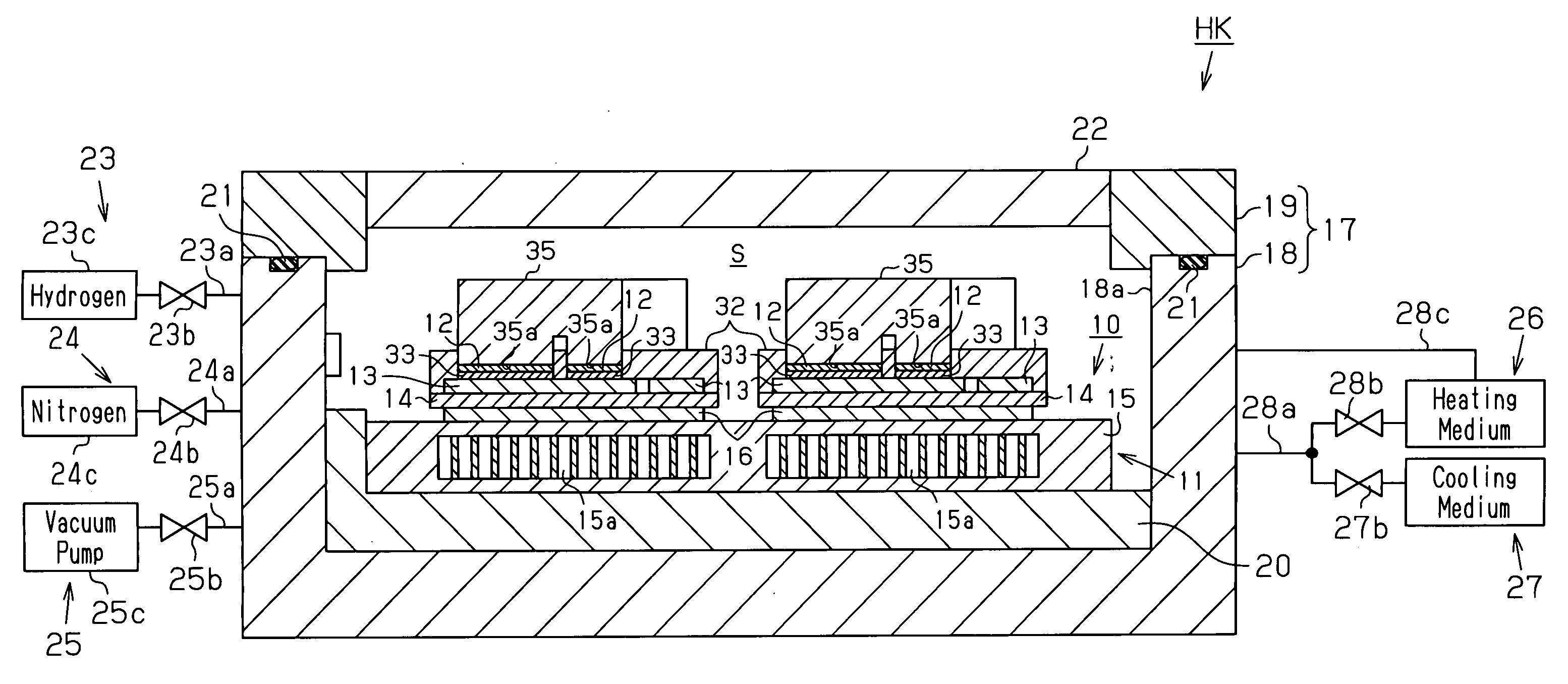
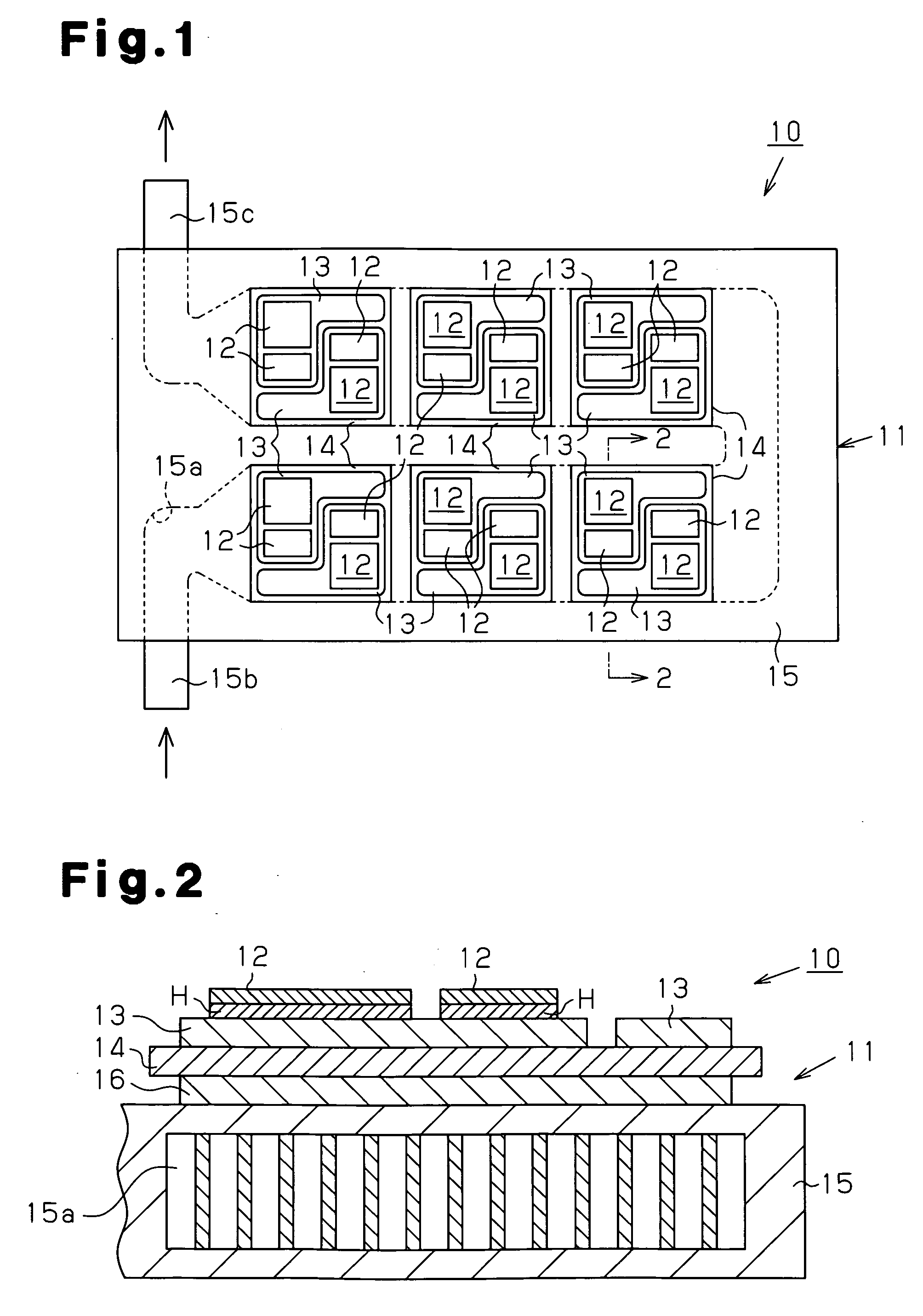
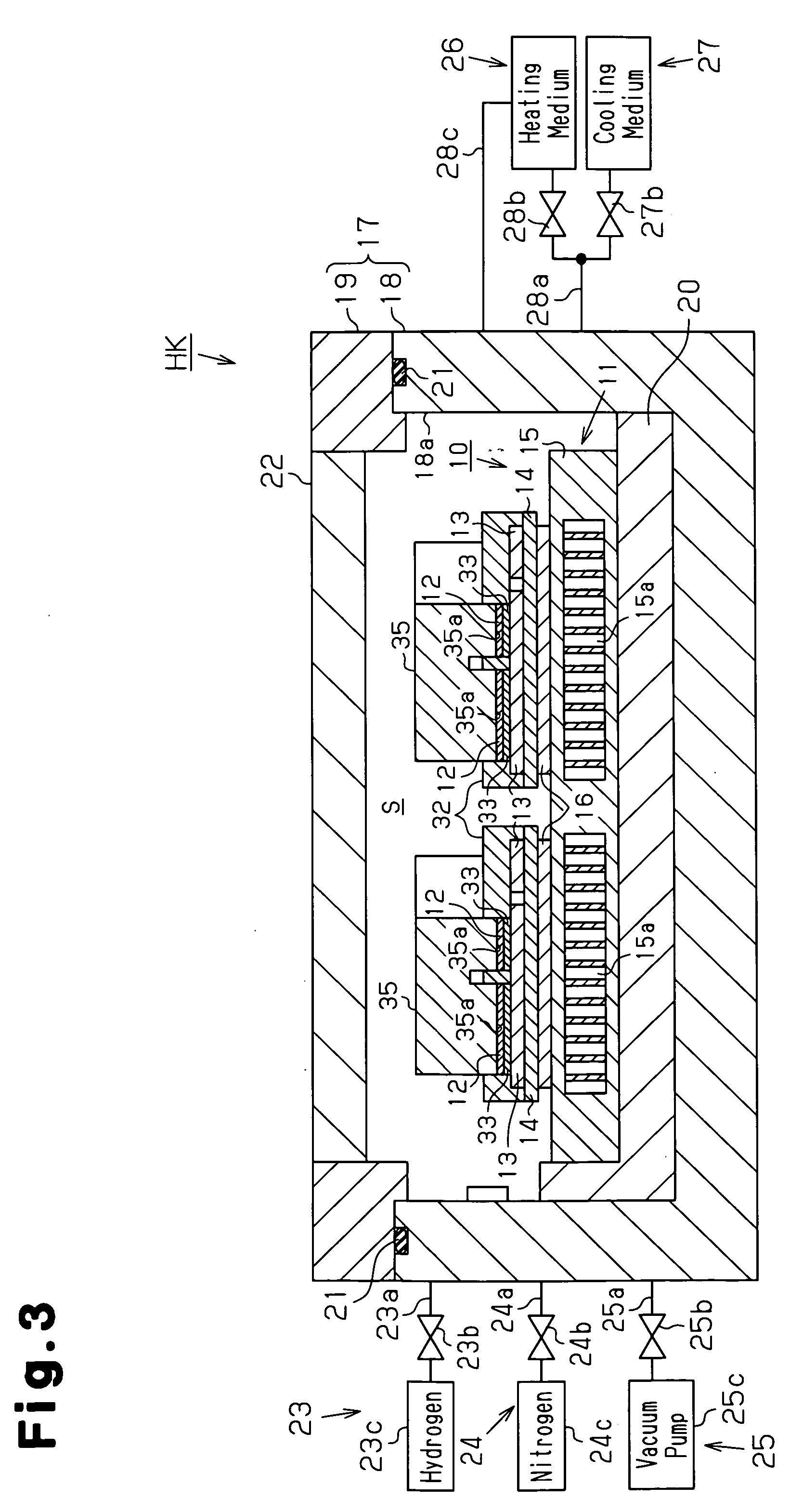
[0023]As shown in FIG. 1, a semiconductor module (semiconductor device) 10 includes a circuit board 11 and a plurality of semiconductor elements 12, which serve as electronic components. The plurality of semiconductor elements 12 are soldered and bonded to the circuit board 11. The circuit board 11 includes a plurality of (six in the present embodiment) ceramic substrates 14, which serve as insulation substrate. Metal circuits 13 are arranged on the surface of each ceramic substrate 14. Four semiconductor elements 12 are soldered to each ceramic substrate 14. A total of twenty-four semiconductor elements 12 are laid out on the semiconductor module 10.

[0024]As shown in FIG. 2, the circuit board 11 includes the ceramic substrates 14 and a metal heat sink 15, which is fixed to the ceramic substrates 14 with a metal plate 16 arranged therebetween. That is, the circuit board 11 is a cooling circuit board. Th...


PUM

PropertyMeasurementUnit
weightaaaaaaaaaa
temperatureaaaaaaaaaa
heat insulatingaaaaaaaaaa

Abstract

A soldering method for soldering an electronic component onto a circuit board is provided. The soldering method uses a cooling circuit board as the circuit board. The cooling circuit board includes an insulation substrate and a metal heat sink. The insulation substrate has a front surface with a metal circuit and a rear surface to which the heat sink is fixed. The heat sink has a refrigerant passage. The electronic component is arranged on the metal circuit with solder in between. A heated heating medium is supplied to the refrigerant passage when heating and melting the solder.

Description

TECHNICAL FIELD[0001]The present invention relates to a soldering method, a semiconductor module manufacturing method, and a soldering apparatus.BACKGROUND ART[0002]When mounting electronic components, such as semiconductor elements, chip resistors, and chip capacitors, on a circuit board, the electronic components are normally bonded to the circuit board with solder. As a method for melting solder when performing soldering, patent document 1 discloses a method that melts solder when a circuit board on which electronic components are mounted by means of solder is conveyed in a reflow furnace. Patent document 2 discloses a method that melts solder by performing high frequency induction heating.[0003]In patent document 1, a soldering apparatus includes a box-shaped carrier, which has an upper portion for holding the board on which the electronic components are mounted, a conveyance mechanism, which conveys the carrier, and a reflow furnace, which is arranged at a predetermined locatio...

Claims


Application Information

Patent Timeline
Patent Type & Authority Applications(United States)
IPC IPC(8): B23K31/02B23K1/20B23K20/10
CPCB23K1/0016H01L2924/1305B23K1/012B23K3/0475B23K3/085B23K3/087B23K2201/42H05K1/0272H05K1/0306H05K3/0061H05K3/3494H05K2201/064H05K2203/101H05K2203/159H01L24/34H01L2224/32225B23K1/002H01L2924/13055H01L2224/40137H01L2924/00H01L2924/15787H01L2924/12042H01L2224/77272H01L2224/83801B23K2101/42H01L24/32H01L24/83H01L24/75H01L2924/00014H05K3/34H01L21/52H01L2224/40225H01L24/36H01L24/40
Inventor KIMBARA, MASAHIKO
Owner TOYOTA IND CORP
Why Eureka
Try Eureka