Chip test apparatus and probe card circuit

Active Publication Date: 2009-09-10
NAN YA TECH
View PDF5 Cites 0 Cited by
  • Summary
  • Abstract
  • Description
  • Claims
  • Application Information

AI Technical Summary

Benefits of technology

[0010]The present invention provides a circuit in probe card, which includes a signal line, a detection probe and a plurality of switch modules. A plurality of test response signals form a plurality of chips to be tested are transmitted on the signal line. The detection probe is coupled to the signal line for receiving the test response signals from the tested chips. In addition, each of the switch modules is respectively coupled to the signal line and the probes to selectively transmit the test response signals from the chips to the signal line such that the chips are able to be tested without disruption caused by an electrical short.

Problems solved by technology

However, in the conventional test apparatus, if any one of the tested chips 102, 104, 106, 108 is damaged, a short circuit phenomenon may occur.
In other words, as long as one of the chips to be tested by the conventional test apparatus is damaged resulting in a short circuit, the test on other chips cannot proceed, and thus those chips will be discarded.

Method used


Image

  • Chip test apparatus and probe card circuit
  • Chip test apparatus and probe card circuit
  • Chip test apparatus and probe card circuit

Examples


Embodiment Construction

[0017]Reference will now be made in detail to the present embodiments of the invention, examples of which are illustrated in the accompanying drawings. Wherever possible, the same reference numbers are used in the drawings and the description to refer to the same or like parts.

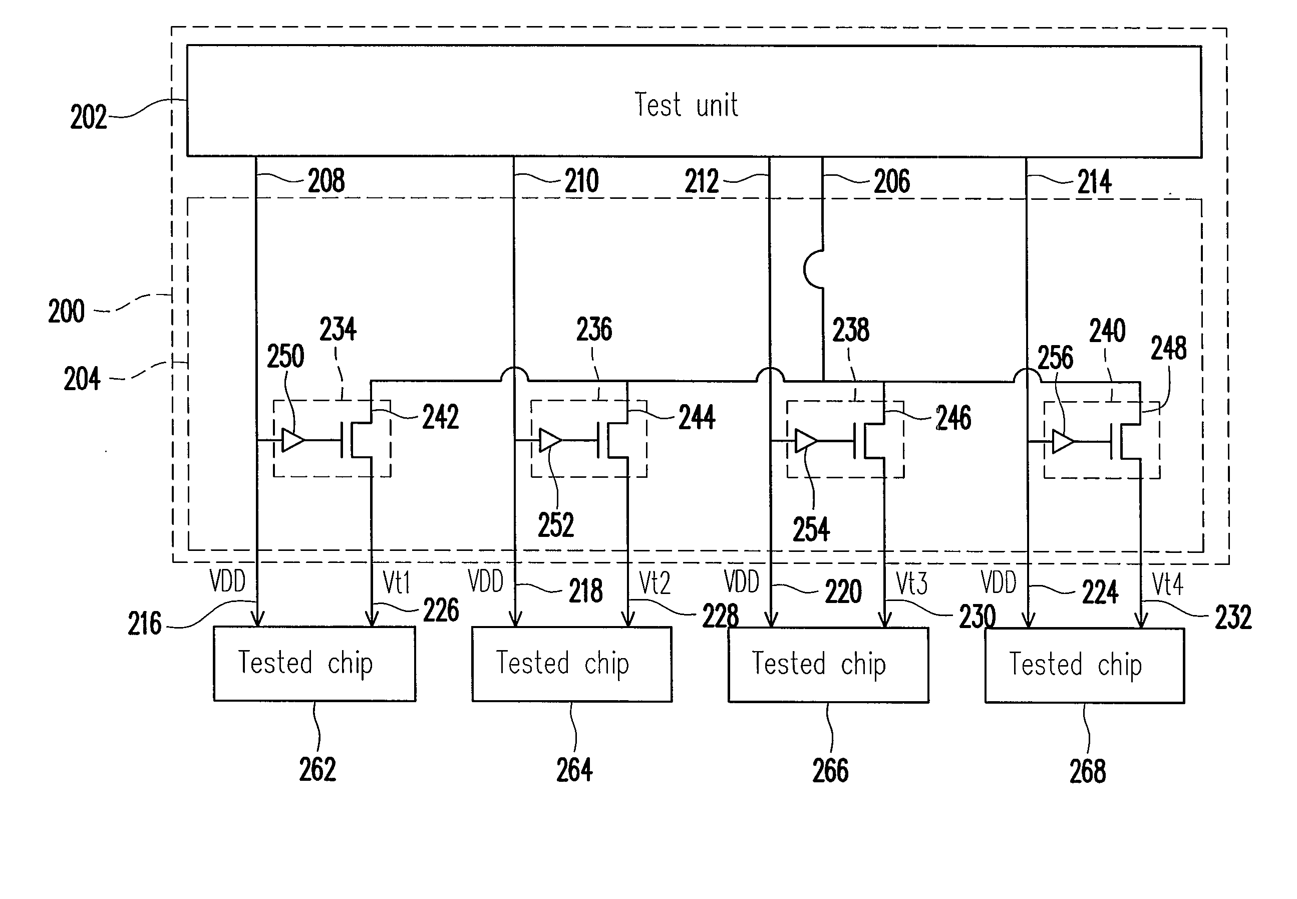
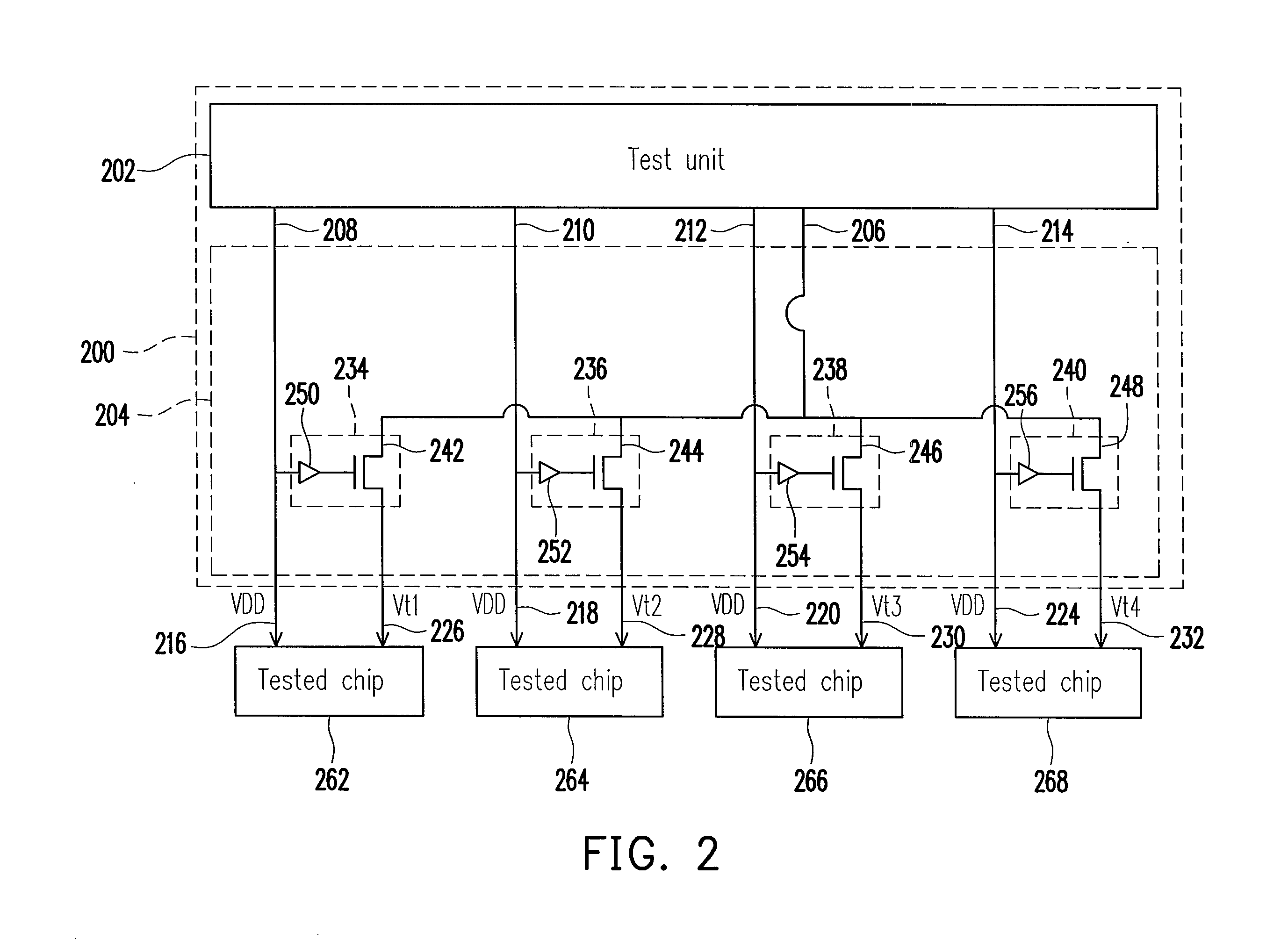
[0018]FIG. 2 is a circuit diagram of a chip test apparatus according to an embodiment of the present invention. Referring to FIG. 2, the chip test apparatus 200 provided by this embodiment may test a plurality of chips, for example, 262, 264, 266, 268 on a wafer at the same time. In this embodiment, the chip test apparatus 200 provides a test power VDD to the tested chips 262, 264, 266, 268. Thus, the tested chips 262, 264, 266, 268 respectively generate test response signals Vt1, Vt2, Vt3, Vt4 to the chip test apparatus 200 after receiving the test power VDD.

[0019]The chip test apparatus 200 includes a test unit 202 and a plurality of probe cards as probe card 204. The test unit 202 is coupled to the probe ca...


PUM


Abstract

A circuit in probe card, which includes a signal line, a detection probe and a plurality of switch modules. A plurality of test response signals form a plurality of chips to be tested are transmitted on the signal line. The detection probe is coupled to the signal line for receiving the test response signals from the tested chips. In addition, each of the switch modules is respectively coupled to the signal line and the probes to selectively transmit the test response signals from the chips to the signal line such that the chips are able to be tested without disruption caused by an electrical short.

Description

CROSS-REFERENCE TO RELATED APPLICATION[0001]This application claims the priority benefit of Taiwan application serial no. 97107731, filed on Mar. 5, 2008. The entirety of the above-mentioned patent application is hereby incorporated by reference herein and made a part of specification.BACKGROUND OF THE INVENTION[0002]1. Field of the Invention[0003]The present invention generally relates to a probe card circuit, and more particularly, to a probe card circuit having a debug function.[0004]2. Description of Related Art[0005]In the current highly-developed technical information society, semiconductor devices take up an important position. However, the semiconductor practitioners have to carry out tests repetitiously or add circuits for testing product quality during the fabrication of semiconductor devices or integrated circuits in order to achieve better quality of the products.[0006]FIG. 1 is a circuit diagram of a conventional chip test apparatus. Referring to FIG. 1, the conventiona...

Claims


Application Information

Patent Timeline
IPC IPC(8): G01R31/02
CPCG01R31/31926
Inventor HSU, CHIA-CHI
Owner NAN YA TECH
Why Eureka
Try Eureka