Microfluid Chip Cleaning

Inactive Publication Date: 2009-09-17
AGILENT TECH INC
View PDF2 Cites 54 Cited by
  • Summary
  • Abstract
  • Description
  • Claims
  • Application Information

AI Technical Summary

Benefits of technology

[0064]When the carrier element is coupled to the substrate in

Problems solved by technology

However, after having used such a microfluidic chip for performing a microfluidic analysis experiment multiple times, it may happen that a gel material or a remnant of an analyt material becomes partially solid and may block at least partially microchannels of the

Method used


Image

  • Microfluid Chip Cleaning
  • Microfluid Chip Cleaning
  • Microfluid Chip Cleaning

Examples


Example

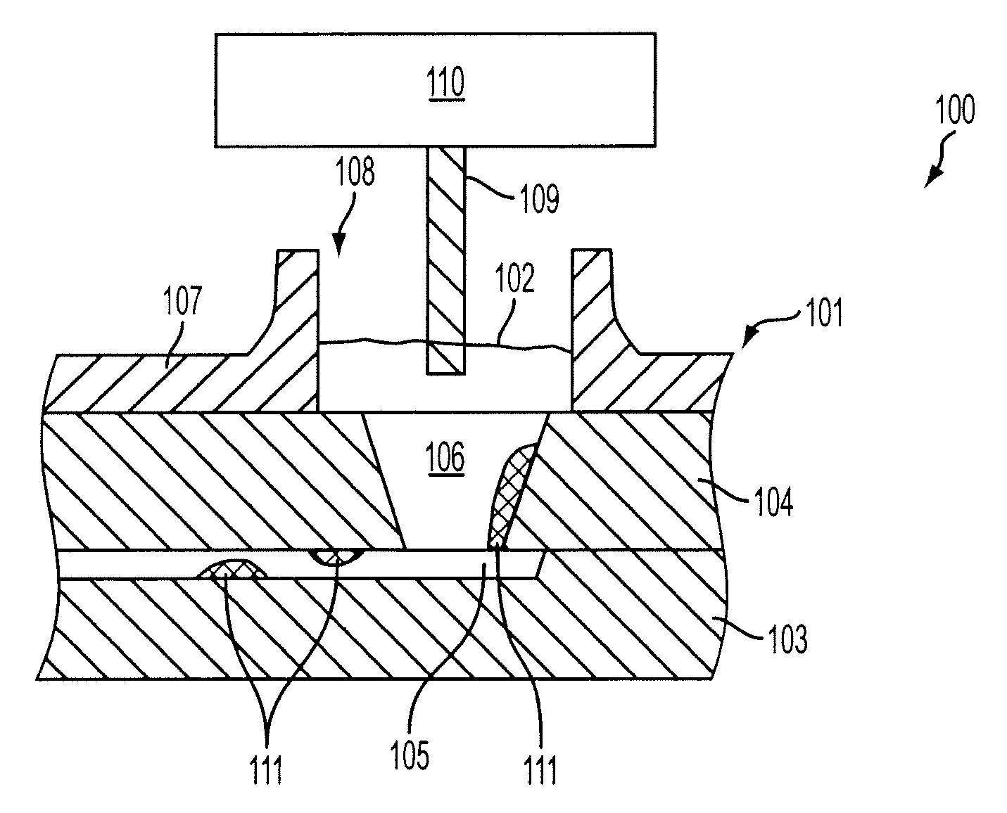
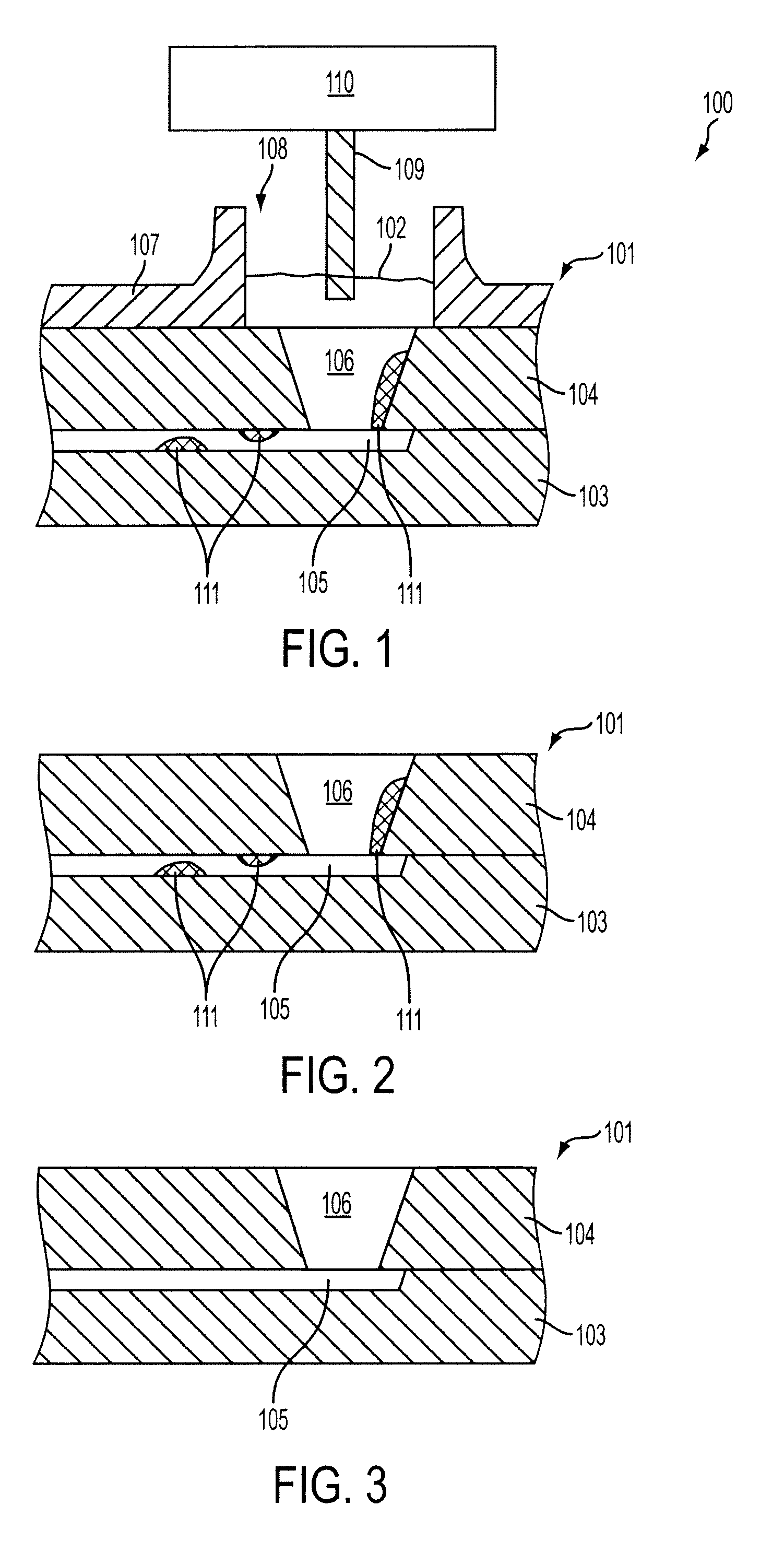
[0075]The illustration in the drawing is schematically.

[0076]In the following, referring to FIG. 1, a fluid separation system 100 for separating components of a fluid according to an exemplary embodiment will be described.

[0077]The fluid separation system 100 comprises a fluid delivering system for delivering fluid 101 to be investigated from containers holding sample material, buffers, and other solutions. Furthermore, an electrophoresis separation system is provided for separating components of the fluid 101. The separation system comprises a microfluidic chip 102, wherein the fluid 101 is insertable in microstructures 105, 106 of the microfluidic chip 102.

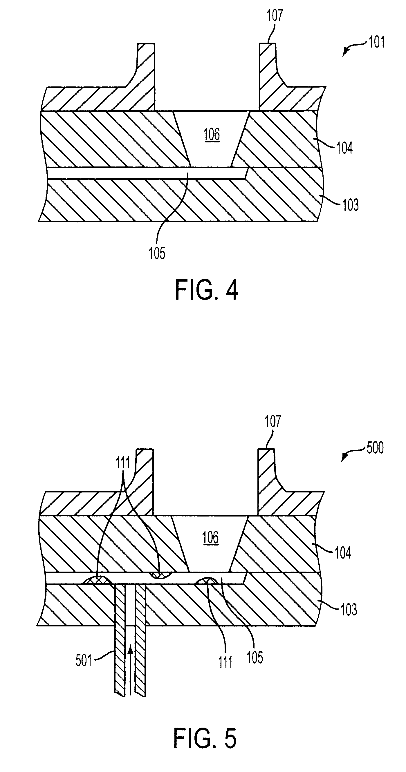
[0078]The microfluidic chip 102 comprises a first glass substrate 103, a second glass substrate 104 bonded with the first glass substrate 103 and a plurality of microstructures 105, 106 formed in the first and in the second glass substrates 103, 104.

[0079]The microstructures 105, 106 of the microfluidic chip 102 include microcha...


PUM

PropertyMeasurementUnit
Temperatureaaaaaaaaaa

Abstract

A method of cleaning a microfluidic chip (101) comprising at least one microstructure (105, 106) containing a material (111), wherein the method comprises removing the material (111) from the at least one microstructure (105, 106) so as to at least partly empty the at least one microstructure (105, 106).

Description

[0001]This application is the National Stage of International Application No. PCT / EP2005 / 054652, filed on 19 Sep. 2005 which designated the United States of America, and which international application was published as Publication No. WO 2007 / 038976.BACKGROUND ART[0002]The present invention relates to microfluidic chip cleaning.[0003]In a microfluidic system for investigating fluidic analyts using microchannels, two glass chips may be provided. In a first glass chip, channels may be etched. In a second glass chip, through holes may be formed. After bonding the first glass chip or substrate to the second glass chip or substrate in such a manner that the through holes are aligned with respect to the channels, fluid may be inserted and pumped or transported using electric forces through the microstructures. The microstructures may be filled with a gel material, for instance in the context of a gel electrophoresis device. After having bonded two substrates, a caddy, that is to say a sup...

Claims


Application Information

Patent Timeline
IPC IPC(8): B08B3/12B01D15/00
CPCB01L3/502707B01L99/00B08B9/00B08B3/12B01L13/02
Inventor BEK, FRITZ
Owner AGILENT TECH INC
Why Eureka
Try Eureka