Metal gate transistor and polysilicon resistor and method for fabricating the same

a technology of metal gate transistor and polysilicon resistor, which is applied in the direction of semiconductor devices, diodes, electrical devices, etc., can solve the problems of polysilicon devices with many drawbacks, depletion region at the interface between the gate and the gate dielectric layer, and depletion

Active Publication Date: 2009-09-24
UNITED MICROELECTRONICS CORP
View PDF8 Cites 78 Cited by
  • Summary
  • Abstract
  • Description
  • Claims
  • Application Information

AI Technical Summary

Problems solved by technology

However, devices fabricated by polysilicon still have many drawbacks.
Gate electrodes fabricated by polysilicon also causes a depletion effect.
As most gate electrodes have a doping concentration of at least 5×10²¹/cm3, the limited doping concentration of polysilicon gates often results in a depletion region at the interface between the gate and the gate dielectric layer.
This depletion region not only thickens the gate dielectric layer, but also lowers t

Method used


Image

  • Metal gate transistor and polysilicon resistor and method for fabricating the same
  • Metal gate transistor and polysilicon resistor and method for fabricating the same
  • Metal gate transistor and polysilicon resistor and method for fabricating the same

Examples


Embodiment Construction

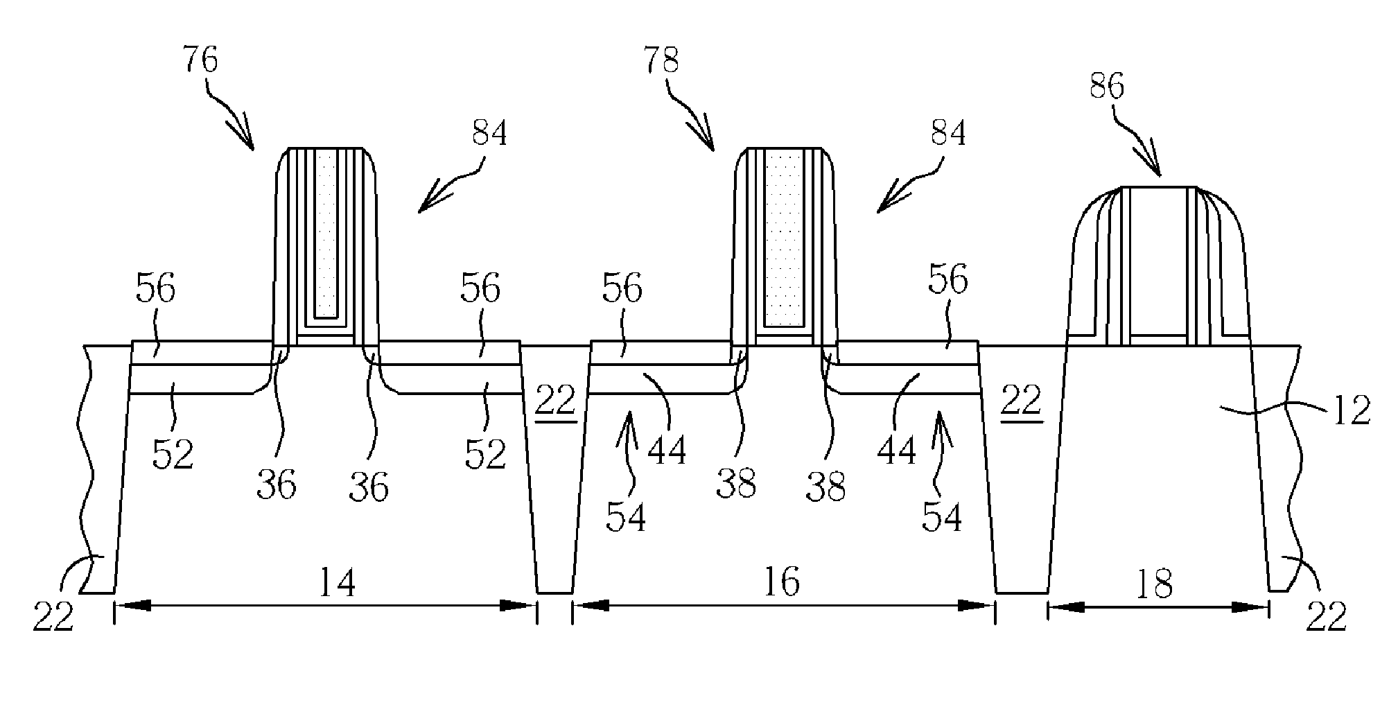
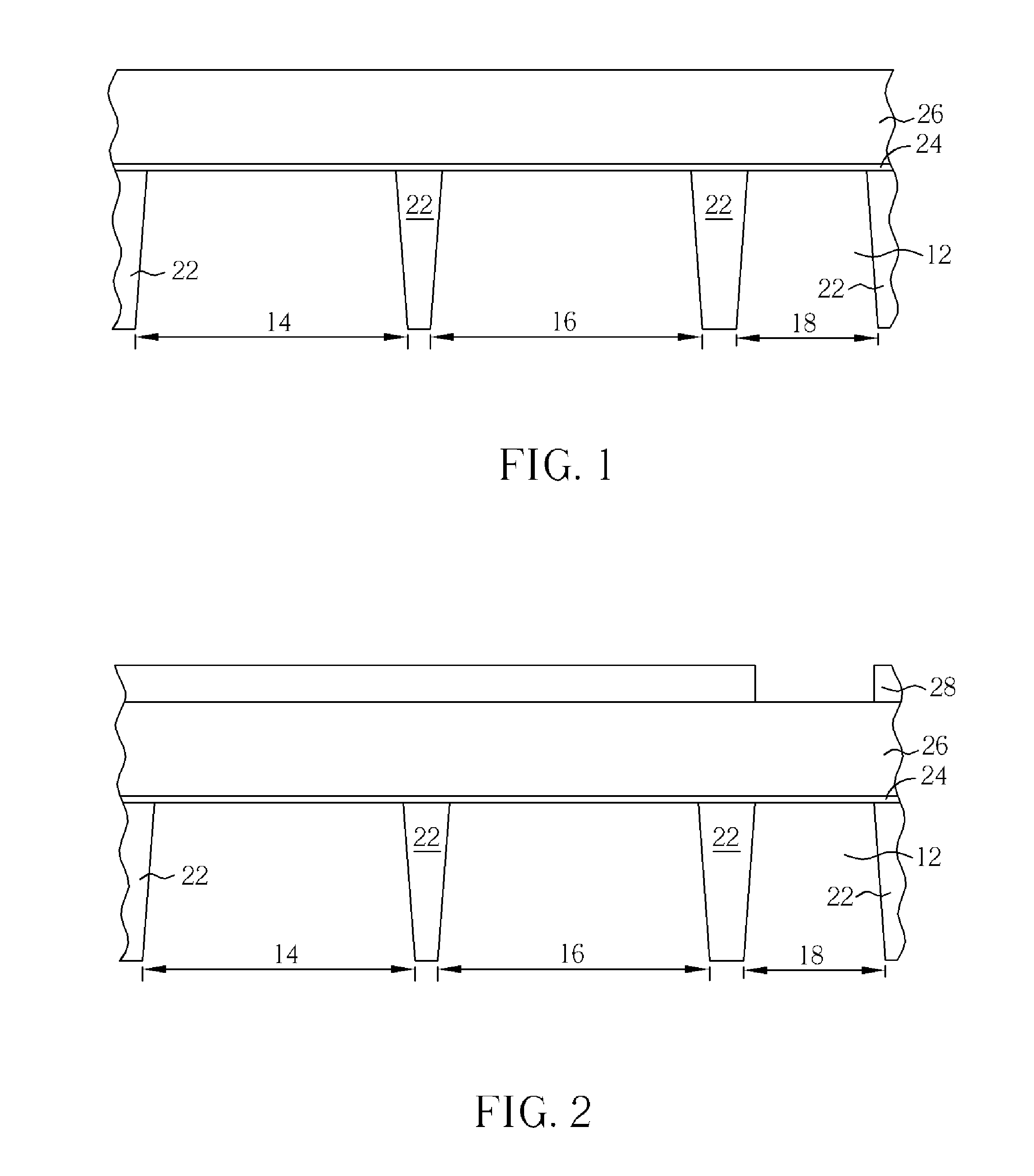
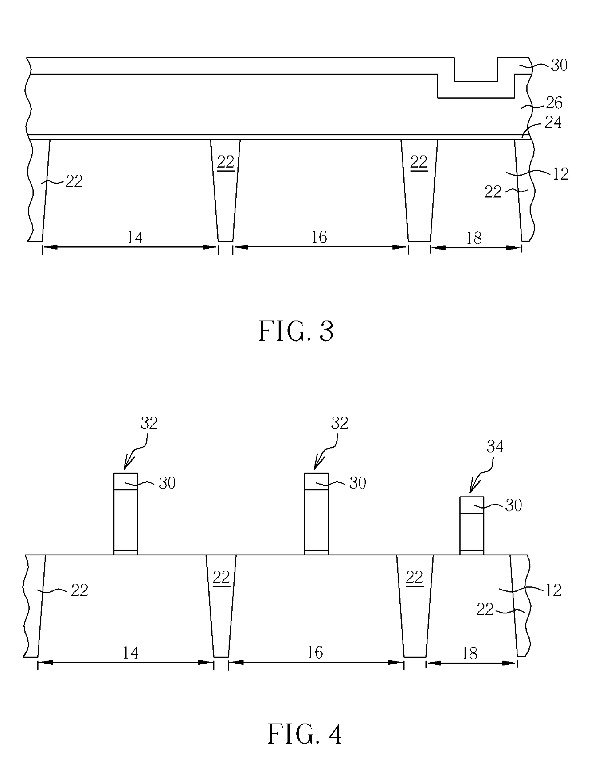
[0015]Referring to FIGS. 1-14, FIGS. 1-14 are perspective views illustrating a method for fabricating a device having metal gate transistors and polysilicon resistor according to a preferred embodiment of the present invention. As shown in FIG. 1, a substrate 12 is first provided. The substrate 12 is preferably a silicon substrate or a silicon-on-insulator (SOI) substrate. A transistor region and a capacitor region 18 are defined in the substrate 12, and a plurality of shallow trench isolations 22 dividing the transistor region and the capacitor region 18 is also formed. In this embodiment, the transistor region includes a NMOS transistor region 14 and a PMOS transistor region 16.

[0016]A gate dielectric layer 24 composed of oxides is formed on the substrate 12, and a polysilicon layer 26 having a thickness of about 1000 angstroms is formed on the gate dielectric layer 24 thereafter. In this embodiment, the polysilicon layer 26 can be composed of undoped polysilicon or polysilicon ha...


PUM


Abstract

A method for fabricating metal gate transistors and a polysilicon resistor is disclosed. First, a substrate having a transistor region and a resistor region is provided. A polysilicon layer is then formed on the substrate to cover the transistor region and the resistor region of the substrate. Next, a portion of the polysilicon layer disposed in the resistor is removed, and the remaining polysilicon layer is patterned to create a step height between the surface of the polysilicon layer disposed in the transistor region and the surface of the polysilicon layer disposed in the resistor region.

Description

BACKGROUND OF THE INVENTION [0001]1. Field of the Invention[0002]The invention relates to a method for fabricating a semiconductor device having a metal gate transistor and a polysilicon resistor, and more particularly, to a method for lowering the height of polysilicon resistor, such that the top of the polysilicon resistor is lower than the top of the metal gate transistor.[0003]2. Description of the Prior Art[0004]In the field of semiconductor fabrication, the use of polysilicon material is diverse. Having a strong resistance for heat, polysilicon materials are commonly used to fabricate gate electrodes for metal-oxide semiconductor transistors. The gate pattern fabricated by polysilicon materials is also used to form self-aligned source / drain regions as polysilicon readily blocks ions from entering the channel region.[0005]However, devices fabricated by polysilicon still have many drawbacks. In contrast to most metal, polysilicon gates are fabricated by semiconductor materials h...

Claims


Application Information

Patent Timeline
IPC IPC(8): H01L29/78H01L21/20H01L21/8234
CPCH01L21/28079H01L21/823807H01L21/823814H01L21/823842H01L29/7833H01L29/4958H01L29/66545H01L29/6659H01L27/0629
Inventor CHEN, YI-WENCHENG, LI-WEIHSU, CHE-HUAYU, CHIH-HAOCHOU, CHENG-HSIENLAI, CHIEN-MINGCHIANG, TIAN-FULIN, CHIEN-TINGMA, GUANG-HWA
Owner UNITED MICROELECTRONICS CORP
Why Eureka
Try Eureka