Ball grid array package system

Active Publication Date: 2009-09-24
STATS CHIPPAC LTD
View PDF18 Cites 27 Cited by
  • Summary
  • Abstract
  • Description
  • Claims
  • Application Information

AI Technical Summary

Problems solved by technology

Issues with respect to the cost of supplying a known good die (KGD) and corresponding fine line and spacing PCB are present.
As the demand for high speed, high performance, and low cost, semiconductor devices are continually increasing in integration density, packages have become more complex.
One problem with placing multiple die within a single package is with additional die, additional possible defects are possible within the package.
Thus, although MCM's have provided increased functionality, yields have decreased as a result of the increased chances for defects.
Solutions to these problems have been long sought but prior developments have not taught or suggested any solutions and, thus, solutions to these problems have long eluded those skilled in the art.

Method used


Image

  • Ball grid array package system
  • Ball grid array package system
  • Ball grid array package system

Examples


Embodiment Construction

[0018]The following embodiments are described in sufficient detail to enable those skilled in the art to make and use the invention. It is to be understood that other embodiments would be evident based on the present disclosure, and that process or mechanical changes may be made without departing from the scope of the present invention.

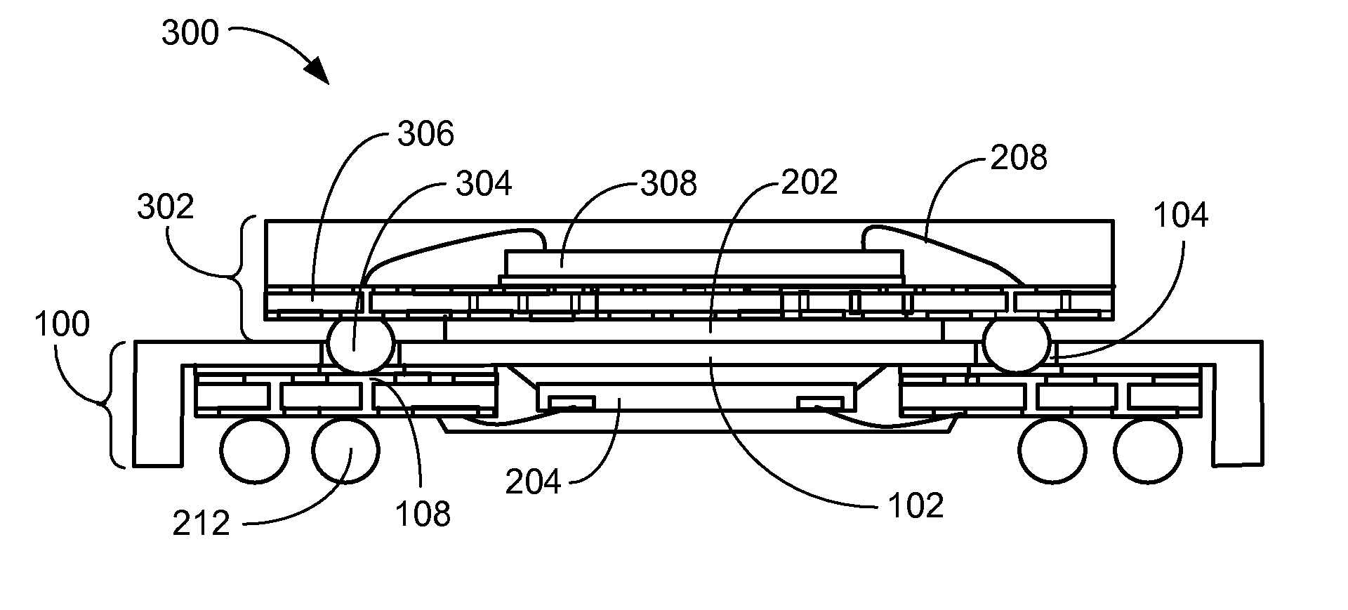
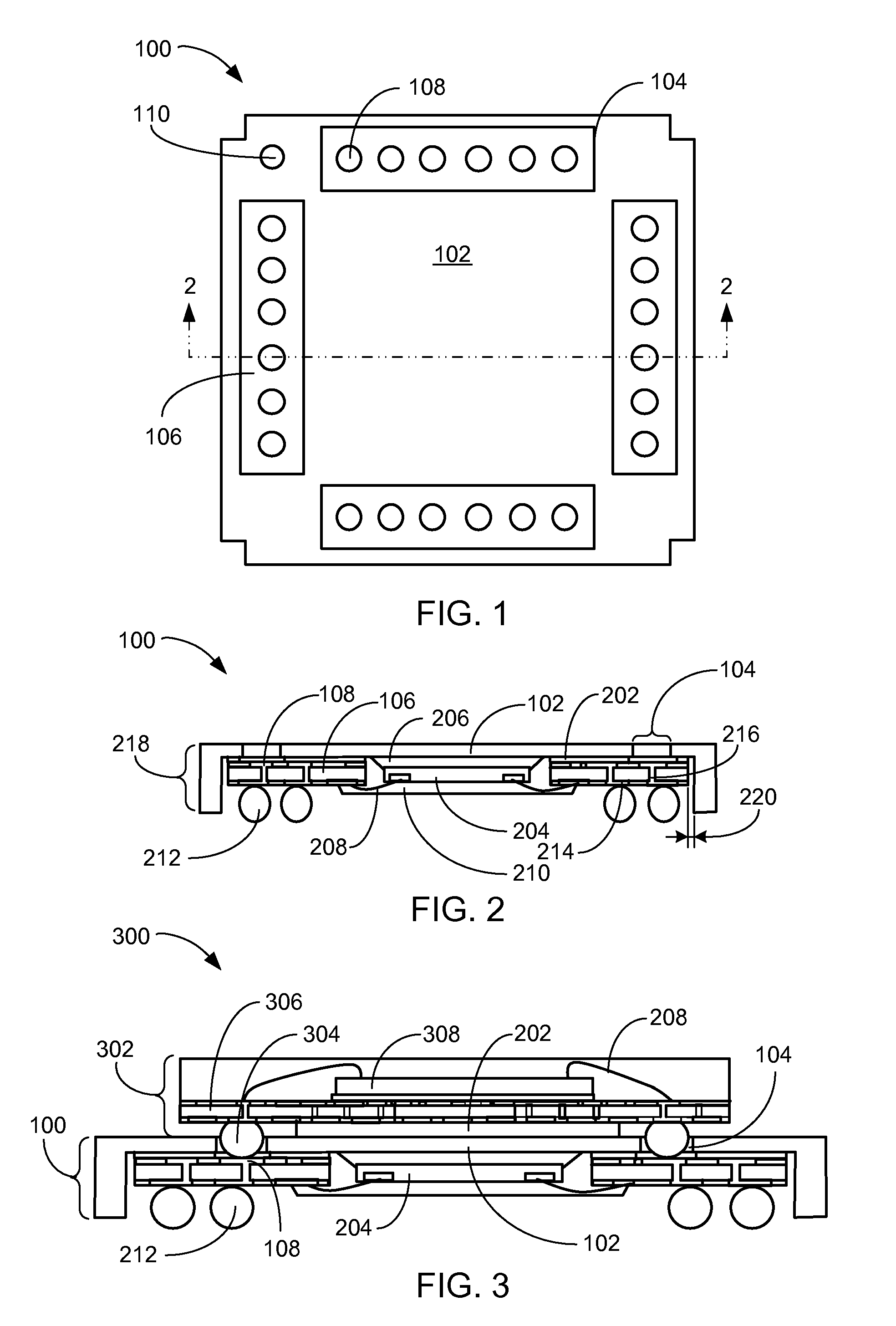
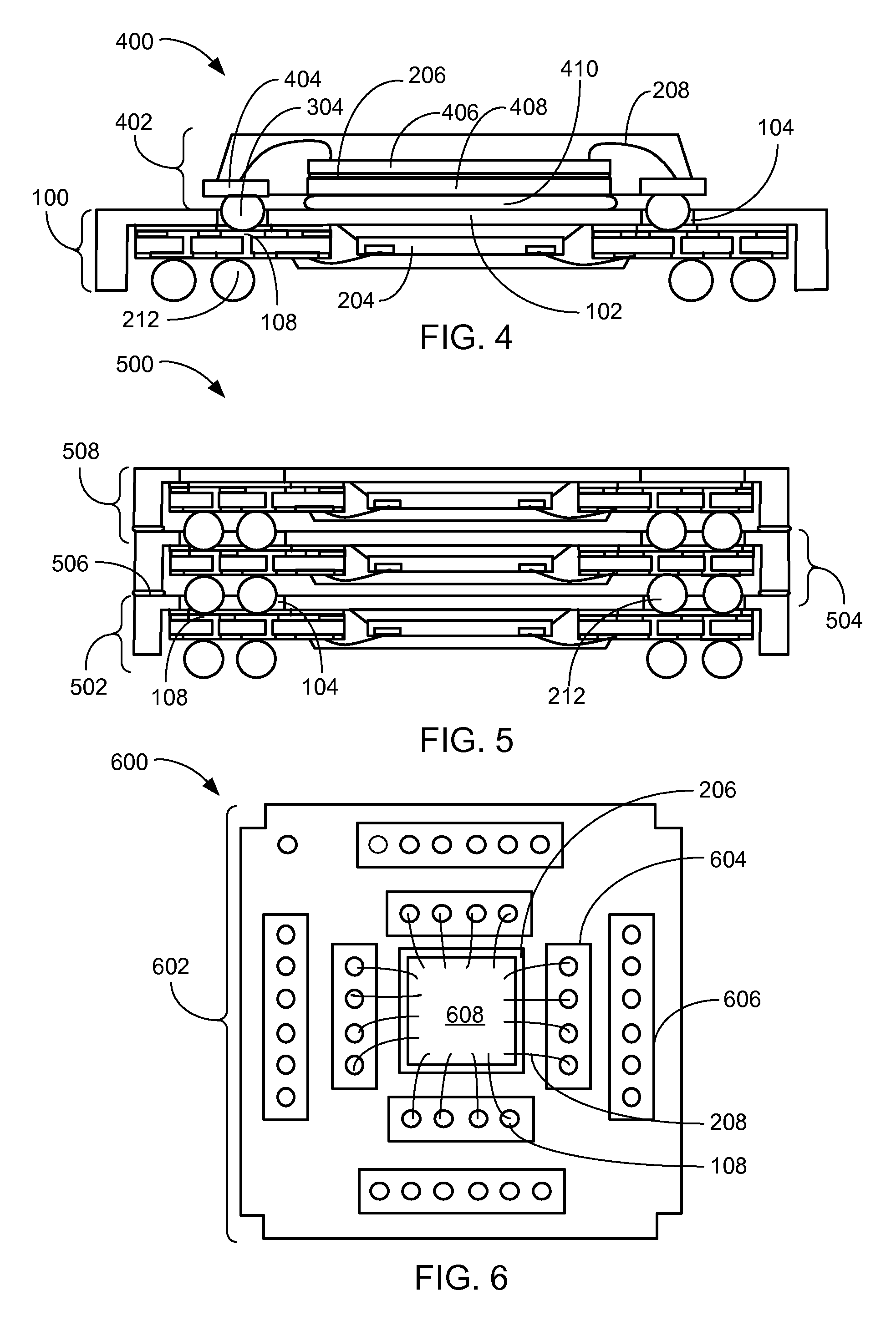
[0019]In the following description, numerous specific details are given to provide a thorough understanding of the invention. However, it will be apparent that the invention may be practiced without these specific details. In order to avoid obscuring the present invention, some well-known circuits, system configurations, and process steps are not disclosed in detail. Likewise, the drawings showing embodiments of the system are semi-diagrammatic and not to scale and, particularly, some of the dimensions are for the clarity of presentation and are shown greatly exaggerated in the drawing FIGs. Where multiple embodiments are disclosed and described, havi...


PUM


Abstract

A ball grid array package system comprising: forming a package base including: fabricating a heat spreader having an access port, attaching an integrated circuit die to the heat spreader, mounting a substrate around the integrated circuit die, and coupling an electrical interconnect between the integrated circuit die and the substrate; and coupling a second integrated circuit package to the substrate through the access port.

Description

TECHNICAL FIELD[0001]The present invention relates generally to integrated circuit packaging, and more particularly to a system for enhancing the capabilities of ball grid array packaging.BACKGROUND ART[0002]A number of different packaging technologies exist for attaching semiconductor devices to a printed circuit board (PCB). Many of today's consumer electronic devices, such as personal video players, video games and hand held computers require a high density of integrated circuits mounted on the PCB. The three packaging technologies include a ball grid array (BGA), chip scale package (CSP), and direct chip attach (DCA). BGA is an older technology relative to CSP and DCA. Theoretically speaking, the most effective packaging technology is DCA. DCA involves the direct attachment of the chip to the PCB without a package, such as a solder-bumped flip chip or wire bonding chip on the board. Issues with respect to the cost of supplying a known good die (KGD) and corresponding fine line a...

Claims


Application Information

Patent Timeline
IPC IPC(8): H01L23/34H01L21/02
CPCH01L23/13H01L2924/07802H01L23/36H01L23/49816H01L25/105H01L2224/48091H01L2224/48227H01L2224/49171H01L2224/73265H01L2924/1433H01L2924/15311H01L2924/19041H01L2924/3025H01L23/3128H01L2224/48247H01L2224/32245H01L2225/1094H01L2225/1058H01L2225/1035H01L2924/3511H01L2224/32225H01L24/49H01L24/48H01L2924/00014H01L2924/00H01L2924/00012H01L24/73H01L2924/14H01L2924/181H01L2224/45099H01L2224/45015H01L2924/207
Inventor CHOW, SENG GUANTAY, LIONEL CHIEN HUI
Owner STATS CHIPPAC LTD
Why Eureka
Try Eureka