Alignment method, tip position detecting device and probe apparatus

a technology of detecting device and probe, which is applied in the direction of measurement device, semiconductor/solid-state device testing/measurement, instruments, etc., can solve the problems of not revealing the detection of the tip of the probe, the difficulty of avoiding such deviation in manufacturing even the same type of probe cards, and the long time required to align the object and the probe card. , to achieve the effect of improving inspection reliability, high accuracy and simplifying the process of detecting the heigh

Active Publication Date: 2009-10-08
TOKYO ELECTRON LTD
View PDF6 Cites 20 Cited by
  • Summary
  • Abstract
  • Description
  • Claims
  • Application Information

AI Technical Summary

Benefits of technology

[0015]In view of the above, the present invention provides an alignment method, a tip position detecting device and a probe apparatus capable of simplifying a process of detecting a height of probes such that an alignment of inspection electrodes of an object to be inspected and the probes can be implemented with a high accuracy within a short period of time, thereby increasing inspection reliability.
[0021]In accordance with a second aspect of the present invention, there is provided a tip position detecting device for use in implementation of electric characteristic inspection of an object to be inspected via electric contact between the object and probes, the tip position detecting device being used to detect tip positions of the probes, wherein the tip position detecting device includes a sensor unit to detect tips of the probes, wherein the sensor unit includes a sensor body, a contact member provided at the sensor body to be vertically movable, and a pressure applying tool to apply a predetermined pressure to the contact member such that the contact member is spaced apart from the sensor body by a predetermined distance, wherein the sensor body includes an elastic supporting device to elastically support the contact member with the predetermined pressure applied by the pressure applying tool, and wherein the contact member is moved downward to the sensor body when it comes into contact with the probes under the predetermined pressure, enabling detection of the tip positions of the probes.
[0023]In accordance with a third aspect of the present invention, there is provided a probe apparatus comprising a movable mounting table on which an object to be inspected is disposed, probes arranged above the mounting table, and a tip position detecting device provided at the mounting table to detect tip positions of the probes, wherein the tip position detecting device includes a sensor unit to detect tips of the probes, wherein the sensor unit includes a sensor body, a contact member provided at the sensor body to be vertically movable, and a pressure applying tool to apply a predetermined pressure to the contact member such that the contact member is spaced apart from the sensor body by a predetermined distance, wherein the sensor body includes an elastic supporting device to elastically support the contact member with the predetermined pressure applied by the pressure applying tool, and wherein the contact member is moved downward to the sensor body when it comes into contact with the probes under the predetermined pressure, enabling detection of the tip positions of the probes.
[0028]In accordance with the aspects of the present invention, it is possible to provide an alignment method, a tip position detecting device and a probe apparatus capable of simplifying a process of detecting a height of probes such that an alignment of inspection electrodes of an object to be inspected and the probes can be implemented with a high accuracy within a short period of time, thereby increasing inspection reliability.

Problems solved by technology

Consequently, a long time is inevitably required to align the object and the probe card.
Moreover, there may be a deviation in manufacturing probe cards and it is difficult to avoid such a deviation in manufacturing even the same type of probe cards.
However, Patent Document 1 does not disclose detection of probe tips as an important alignment factor.
However, a depth of the needle marks should be detected to detect a height of probe tips and, thus, it is difficult to detect the height of the probe tips with a high accuracy.
Therefore, a long time is inevitably required to detect the tip positions of the probes 5A.

Method used


Image

  • Alignment method, tip position detecting device and probe apparatus
  • Alignment method, tip position detecting device and probe apparatus
  • Alignment method, tip position detecting device and probe apparatus

Examples


first embodiment

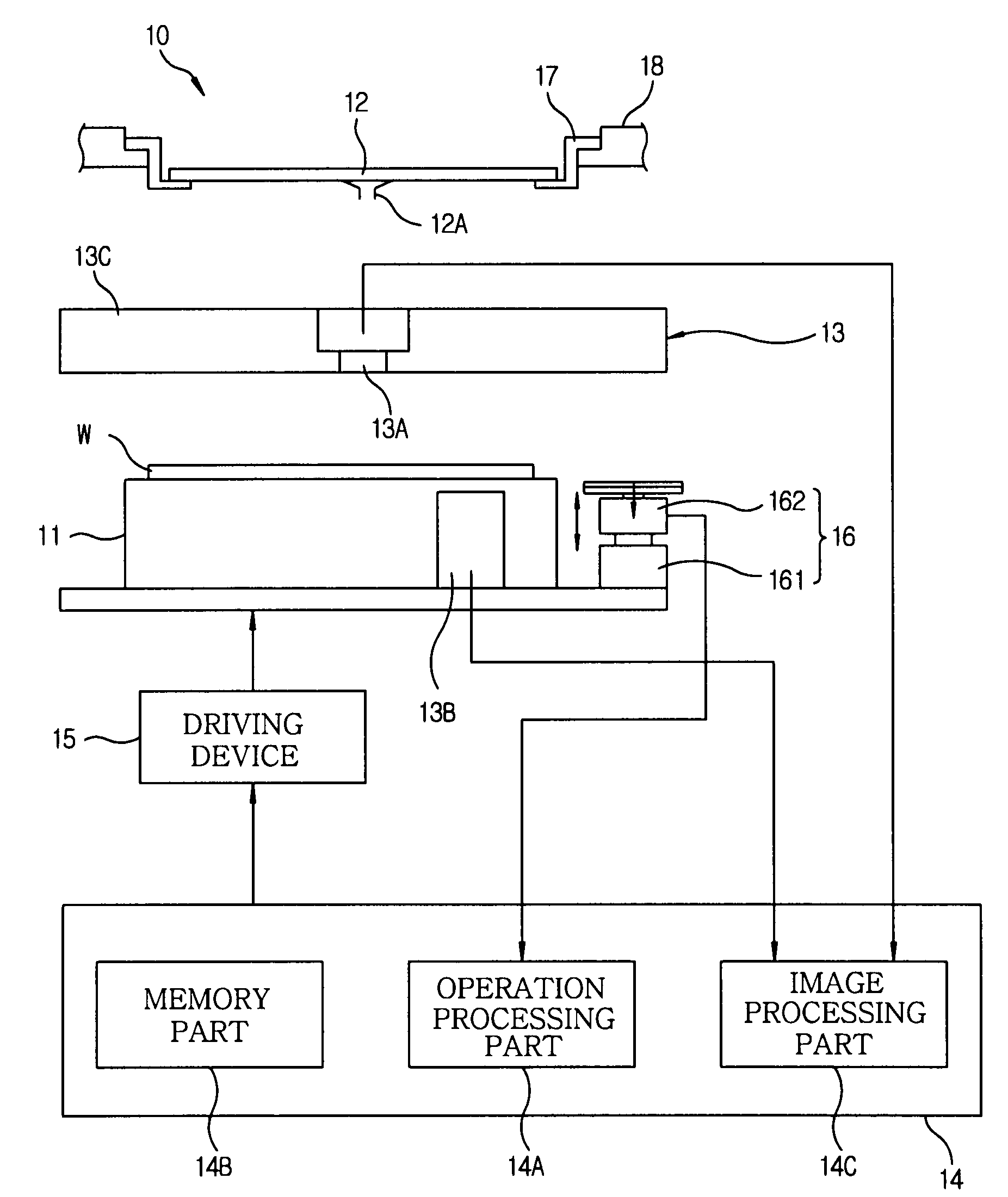
[0041]First, a probe apparatus in accordance with the present embodiment will be described with reference to FIG. 1. The probe apparatus 10 of the present embodiment, as shown in FIG. 1, includes a movable wafer chuck 11 on which a semiconductor wafer W serving as an object to be inspected is mounted, a probe card 12 arranged above the wafer chuck 11, an alignment device 13 which implements an alignment of a plurality of probes 12A of the probe card 12 and the semiconductor wafer W mounted on the wafer chuck 11, and a controller 14 which controls components such as the wafer chuck 11 and the alignment device 13. The alignment device 13 is operated under control of the controller 14 to align electrode pads of the semiconductor wafer W mounted on the wafer chuck 11 and the probes 12A of the probe card 12. Then, the probes 12A are made into electric contact with the corresponding electrode pads, thereby conducting inspection of electric characteristics of the semiconductor wafer W.

[004...

second embodiment

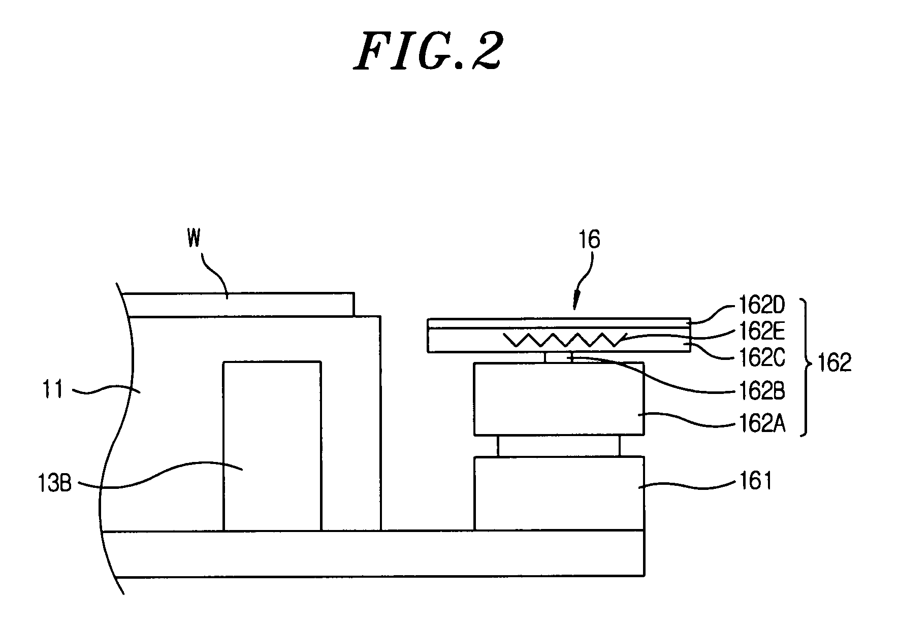
[0072]In the above-described probe apparatus 10 of the first embodiment, the soft member 162D of the tip position detecting device 16 is made of semi-transparent synthetic resin. Further, as described above, the soft member 162D has a limit to have a uniform thickness due to a variation in thickness and is deteriorated in smoothness after removal of the needle marks. Moreover, the soft member 162D may be pricked with the tips of the probes 12A upon detection of the tips of the probes 12A. Thus, it reduces detection accuracy of the tip positions of the probes 12A.

[0073]To solve the above-described problems, as shown in FIG. 8, the probe apparatus of the second embodiment has a feature in that the cylinder device of the first embodiment is divided into a cylinder device serving as a tip position detecting part to detect a height of the tips of the probes 12A and a cylinder device for a soft member (hereinafter, referred to as a transfer sheet in this embodiment) serving as a needle ma...

third embodiment

[0079]As shown in FIG. 9A, a tip position detecting device 26 of the probe apparatus of the third embodiment includes, as a main component, e.g., a sensor unit 27 adapted to detect tips of the probes 12A. The sensor unit 27 includes a sensor body 271, a contact member 272 provided at the sensor body 271 to be vertically movable, and a pressure applying tool (electric regulator) 273 which applies a predetermined pressure to the contact member 272 such that the contact member 272 is spaced apart from the sensor body 271 by a predetermined distance. Under the predetermined pressure, the contact member 272 is moved to come into contact with the probes 12A and, then, is moved to the sensor body 271 due to a contact with the probes 12A, enabling detection of tip positions of the probes 12A. The sensor body 271 is constructed as an elastic supporting device (cylinder device) to elastically support the contact member 272 by the predetermined pressure. The electric regulator 273 is adapted t...


PUM


Abstract

An alignment method is used in implementation of electric characteristic inspection of an object to be inspected via electric contact between the object disposed on a movable mounting table and probes. The alignment method includes detecting tip positions of the probes by using the tip position detecting device, detecting the tip positions of the probes, previously detected by the tip position detecting device, by using the second imaging unit, transferring needle marks of the probes onto a soft member provided at the tip position detecting device by allowing the probes to come into contact with the soft member, detecting the needle marks of the probes formed on the soft member by using the first imaging unit, and detecting inspection electrodes of the object corresponding to the probes by using the first imaging unit.

Description

FIELD OF THE INVENTION [0001]The present invention relates to an alignment method, a tip position detecting device and a probe apparatus for use in implementation of electric characteristic inspection of an object to be inspected, such as a semiconductor wafer. More particularly, the present invention relates to an alignment method, a tip position detecting device and a probe apparatus, capable of implementing alignment of an object to be inspected and a plurality of probes with a high accuracy, thereby increasing inspection reliability.BACKGROUND OF THE INVENTION [0002]When electric characteristic inspection is performed on an object to be inspected, such as a semiconductor wafer, by using a plurality of probes, for example, tips of the probes provided at a probe card are imaged by using a camera to detect tip positions of the probes, and the probes are made into contact with electrode pads of the object, thereby implementing the inspection. The detection of the tip positions of th...

Claims


Application Information

Patent Timeline
Patent Type & Authority Applications(United States)
IPC IPC(8): G01R31/02G01B11/00
CPCG01R31/2891H01L22/00
Inventor YAMADA, HIROSHISUZUKI, MASARUWATANABE, TETSUJIKAWAJI, TAKESHI
Owner TOKYO ELECTRON LTD
Why Eureka
Try Eureka