Minimizing Power Variations In Laser Sources

a technology of laser source and power variation, which is applied in the field of semiconductor lasers, can solve the problems of green power change, output power variation, and color balance errors of projected images, and achieve the effect of narrowing the wavelength fluctuations of semiconductor lasers and minimizing laser wavelength variations in semiconductor lasers

Inactive Publication Date: 2009-10-08
CORNING INC
View PDF7 Cites 9 Cited by
  • Summary
  • Abstract
  • Description
  • Claims
  • Application Information

AI Technical Summary

Benefits of technology

[0007]For example, according to one embodiment of the present invention, a method of minimizing laser wavelength variations in a semiconductor laser is provided. According to the method, a projected laser image is generated utilizing an output beam of the semiconductor laser. A gain current control signal is generated by a laser feedback loop to control the gain section of the semiconductor laser. Wavelength fluctuations of the semiconductor laser are narrowed by incorporating a wavelength recovery operation in a drive current of the semiconductor laser and by initiating the wavelength recovery operations as a function of the gain current control signal or a wavelength-converted output intensity error signal.

Problems solved by technology

Mode hopping and uncontrolled large wavelength variations within the laser cavity can also lead to output power variations because the bandwidth of a PPLN SHG device is often very small.
In laser projection systems, in particular, mode hops are particularly problematic because they can generate instantaneous changes in power that will be readily visible as defects in specific locations in the image.
In typical RGB projection systems that utilize wavelength conversion devices variations in IR power from any of the aforementioned sources can cause green power to change and create errors in the color balance of the projected image.

Method used


Image

  • Minimizing Power Variations In Laser Sources
  • Minimizing Power Variations In Laser Sources
  • Minimizing Power Variations In Laser Sources

Examples


Embodiment Construction

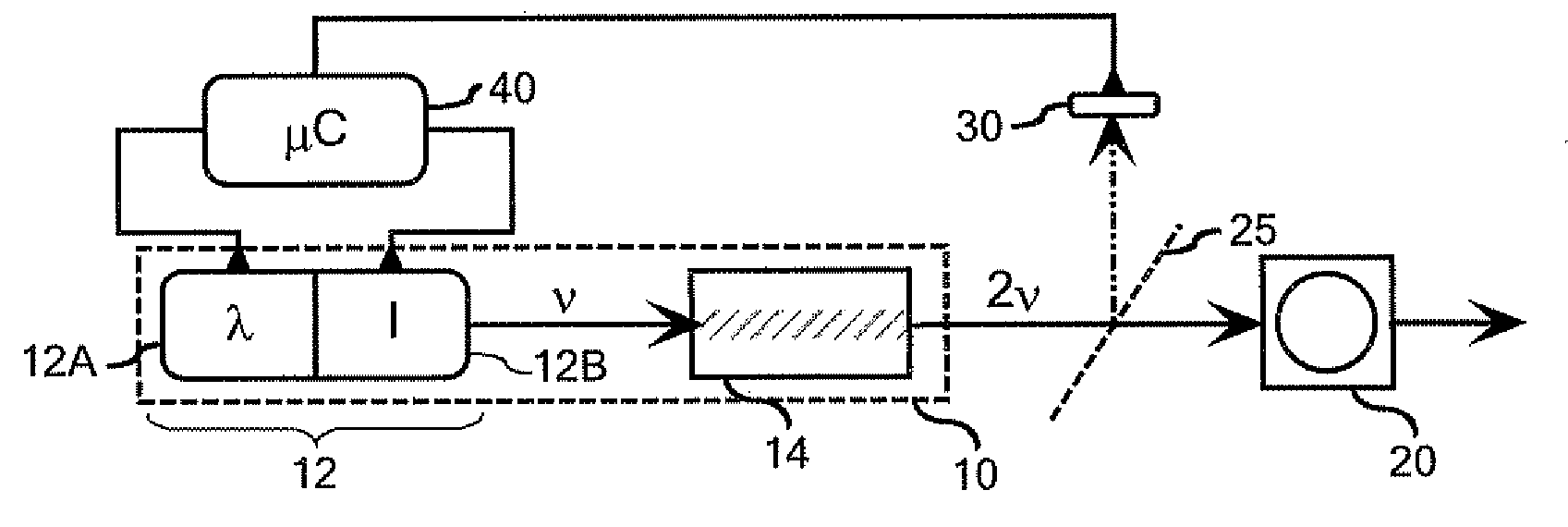
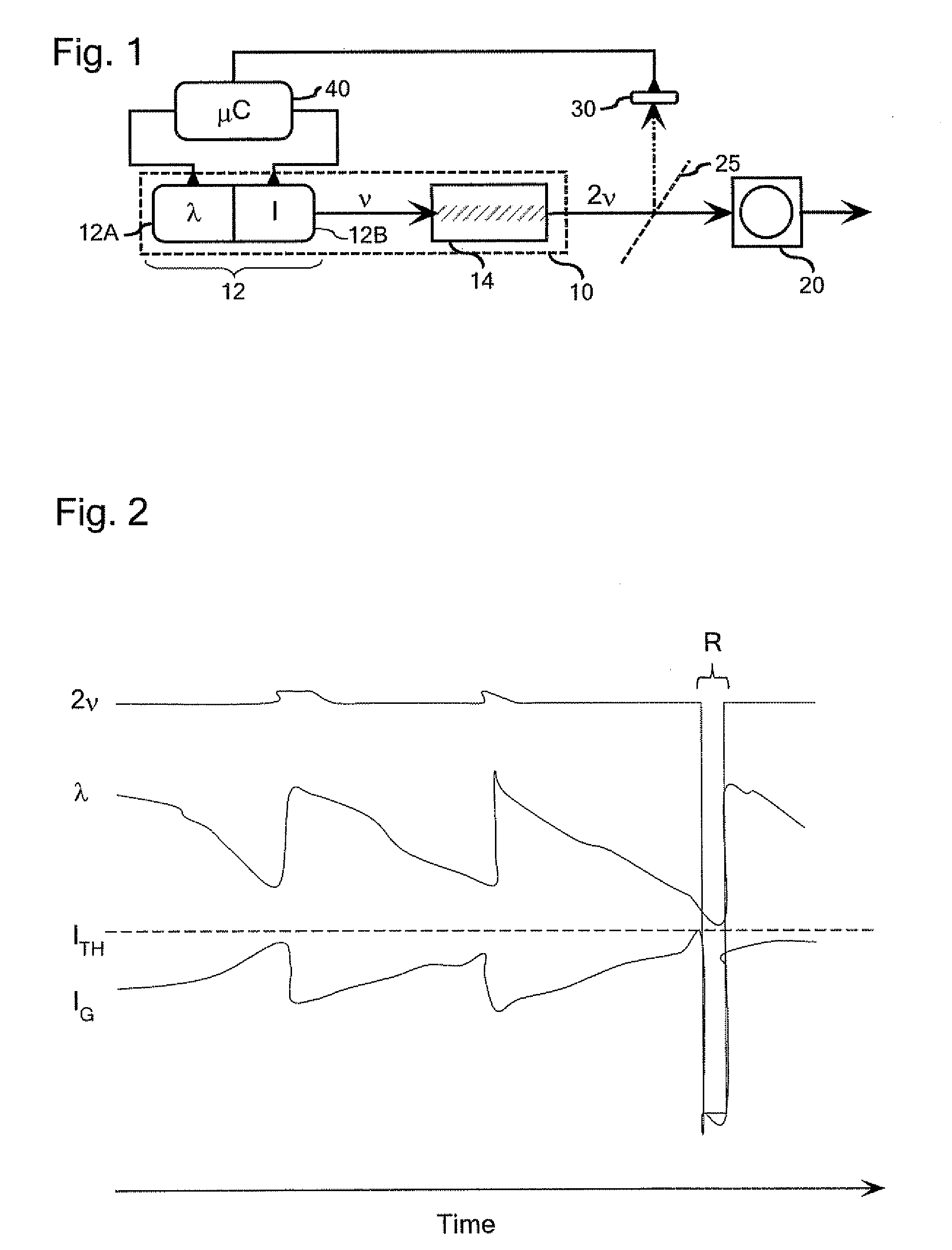
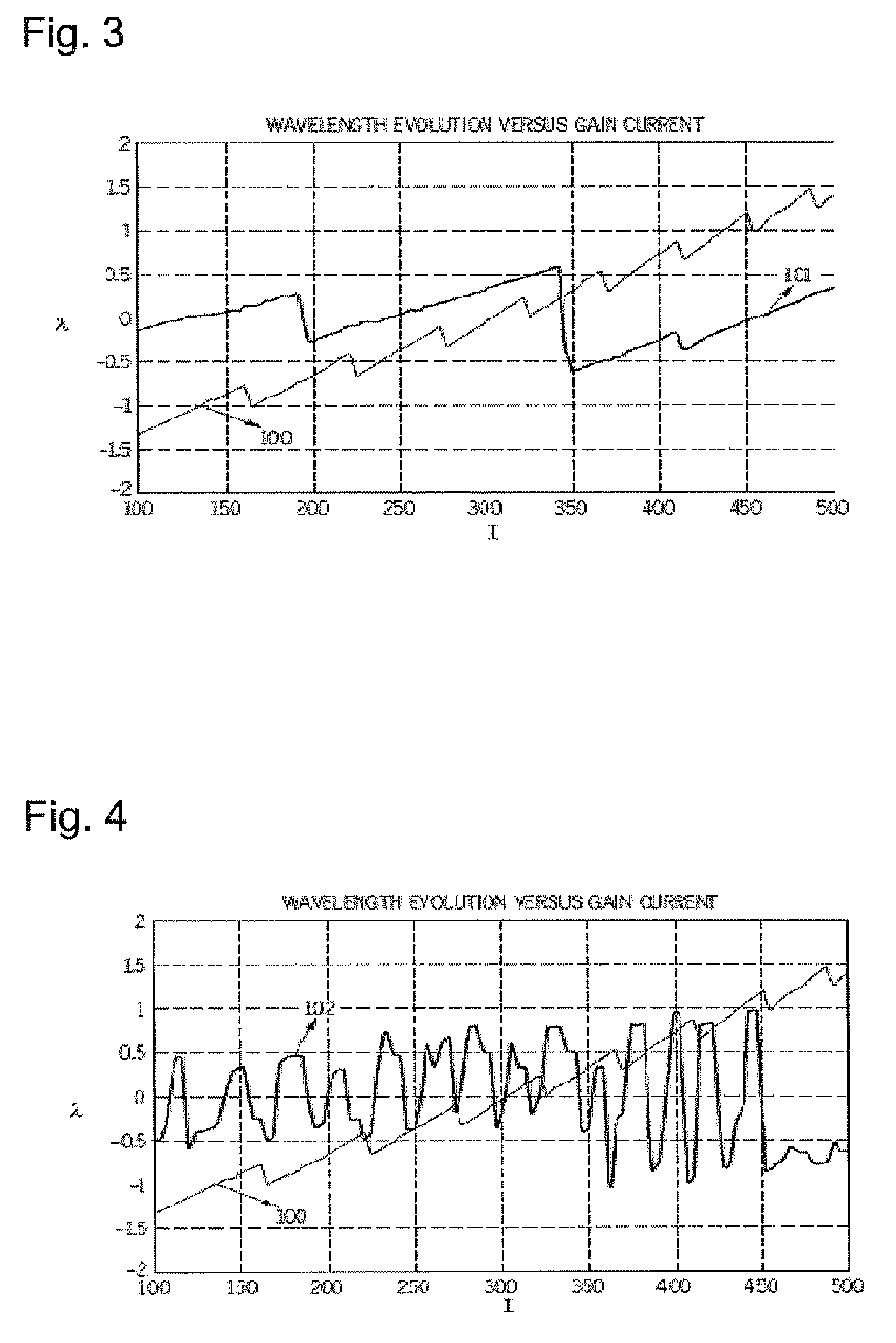
[0021]Referring to FIG. 1, the concepts of the present invention may be conveniently illustrated with general reference to a laser source 10 comprising a two-section DBR-type semiconductor laser 12, although the concepts of the present invention can be executed in the context of various types of semiconductor lasers, the design and operation of which is described generally above and is taught in readily available technical literature relating to the design and fabrication of semiconductor lasers. In the context of a frequency-doubled light source of the type illustrated in FIG. 1, the DBR laser 12 is optically coupled to a light wavelength conversion device 14. The light beam emitted by the semiconductor laser 12 can be either directly coupled into the waveguide of the wavelength conversion device 14 or can be coupled through collimating and focusing optics or some other type of suitable optical element or optical system. The wavelength conversion device 14 converts the incident lig...


PUM


Abstract

The present invention relates generally to semiconductor lasers and laser projection systems. According to one embodiment of the present invention, a projected laser image is generated utilizing an output beam of the semiconductor laser. A gain current control signal is generated by a laser feedback loop to control the gain section of the semiconductor laser. Wavelength fluctuations of the semiconductor laser are narrowed by incorporating a wavelength recovery operation in a drive current of the semiconductor laser and by initiating the wavelength recovery operations as a function of the gain current control signal or an optical intensity error signal. Additional embodiments are disclosed and claimed.

Description

CROSS REFERENCE TO RELATED APPLICATIONS[0001]The present application is a Continuation-In-Part of U.S. patent application Ser. No. 12 / 080,852, filed Apr. 7, 2008. The present application is also related to copending and commonly assigned U.S. patent application Ser. No. 11 / 549,856 filed Oct. 16, 2006 (D 20106), but does not claim priority thereto.BACKGROUND OF THE INVENTION[0002]The present invention relates generally to semiconductor lasers and, more particularly, to schemes for minimizing laser power variations by controlling photon density in the laser cavity of the semiconductor laser. The present invention also relates to laser controllers and laser projection systems programmed according to the present invention.SUMMARY OF THE INVENTION[0003]The present invention relates generally to semiconductor lasers, which may be configured in a variety of ways. For example and by way of illustration, not limitation, short wavelength sources can be configured for high-speed modulation by ...

Claims


Application Information

Patent Timeline
Patent Type & Authority Applications(United States)
IPC IPC(8): H01S3/13
CPCH01S5/0092H01S5/06255H01S5/06256H04N9/3161H01S5/0687H04N9/3129H01S5/06835
Inventor BAUCO, ANTHONY SEBASTIANBUTLER, DOUGLAS LLEWELLYNHU, MARTIN HAIPIKULA, DRAGANRICKETTS, DANIEL OHEN
Owner CORNING INC
Why Eureka
Try Eureka