Wavelength control in semiconductor lasers

a technology of semiconductor lasers and wavelengths, applied in semiconductor lasers, laser details, color television details, etc., can solve the problem of the output wavelength of a semiconductor laser moving outside of the allowable bandwidth, and achieve the effect of minimizing laser wavelength variations in a semiconductor laser

Inactive Publication Date: 2008-04-17
CORNING INC
View PDF6 Cites 30 Cited by
  • Summary
  • Abstract
  • Description
  • Claims
  • Application Information

AI Technical Summary

Benefits of technology

[0007]According to one embodiment of the present invention, a method of minimizing laser wavelength variations in a semiconductor laser is provided. According to the method, one or more of the laser drive currents is configured to comprise a drive portion and a wavelength recovery portion. The wavelength recovery portion of the drive current comprises a recovery amplitude IR that is distinct from the drive amplitude ID and a recovery duration tR that is less than the drive duration tD. The recovery amplitude IR and duration tR are sufficient to recover the desired carrier density distribution distorted by gain compression effects prior to recovery. For example, and not by way of limitation, it is contemplated that gain compression effects may arise as a result of spectral hole burning and spatial hole burning in the laser cavity. The resulting drive current comprising the drive portion and the wavelength recovery portion is used to operate the laser. Due to the recovery of the carrier density distribution, some of the adverse phenomena such as large wavelength drift, abnormal wavelength mode hops, and hysteresis are eliminated.

Problems solved by technology

Mode hopping and uncontrolled large wavelength variations within the laser cavity can cause the output wavelength of a semiconductor laser to move outside of this allowable bandwidth during operation.
In laser projection systems, in particular, mode hops are particularly problematic because they can generate instantaneous changes in power that will be readily visible as defects in specific locations in the image.

Method used


Image

  • Wavelength control in semiconductor lasers
  • Wavelength control in semiconductor lasers
  • Wavelength control in semiconductor lasers

Examples


Embodiment Construction

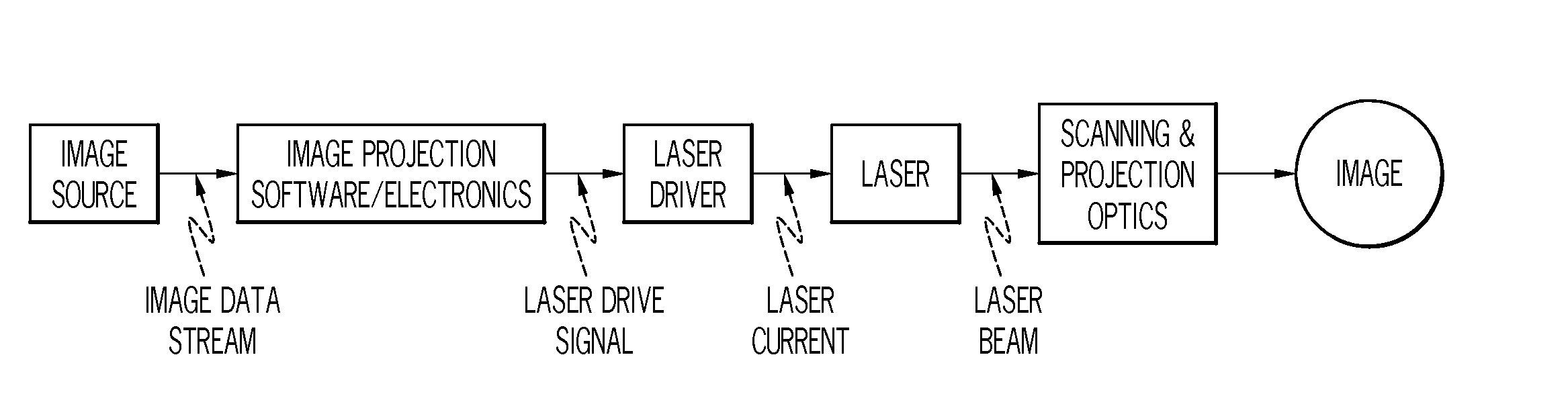
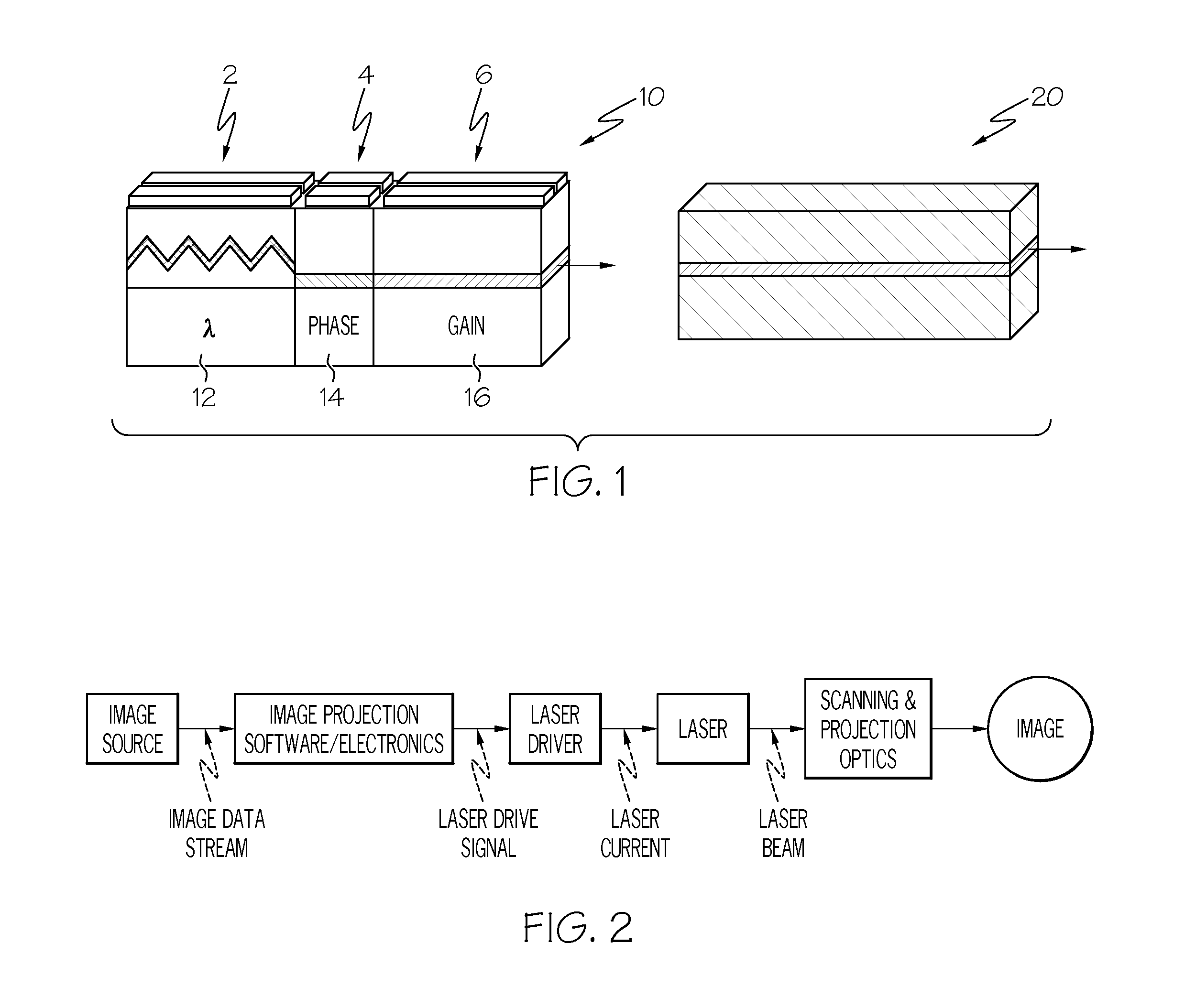
[0016]Although the specific structure of the various types of semiconductor lasers in which the concepts of the present invention can be incorporated is taught in readily available technical literature relating to the design and fabrication of semiconductor lasers, the concepts of the present invention may be conveniently illustrated with general reference to a three-section DBR-type semiconductor laser 10 illustrated schematically in FIG. 1. In FIG. 1, the DBR laser 10 is optically coupled to light wavelength conversion device 20. The light beam emitted by the semiconductor laser 10 can be either directly coupled into the waveguide of the wavelength conversion device 20 or can be coupled through collimating and focusing optics or some other type of suitable optical element or optical system. The wavelength conversion device 20 converts the incident light into higher harmonic waves and outputs the converted signal. This type of configuration is particularly useful in generating shor...


PUM


Abstract

The present invention relates generally to semiconductor lasers and laser scanning systems and, more particularly, to schemes for controlling wavelength in semiconductor lasers. According to one embodiment of the present invention, a method of minimizing laser wavelength variations in a semiconductor laser is provided. According to the method, one or more of the laser drive currents is configured to comprise a drive portion and a wavelength recovery portion. The wavelength recovery portion of the drive current comprises a recovery amplitude IR that is distinct from the drive amplitude ID and a recovery duration tR that is less than the drive duration tD. The recovery amplitude IR and duration tR are sufficient to recover carrier density distribution distorted by gain compression effects prior to recovery. Additional embodiments are disclosed and claimed.

Description

CROSS REFERENCE TO RELATED APPLICATIONS[0001]The present application is related to copending and commonly assigned U.S. patent application Ser. No. ______(D20254 & D20293) Ser. No. ______, but does not claim priority thereto.BACKGROUND OF THE INVENTION[0002]The present invention relates generally to semiconductor lasers and, more particularly, to schemes for minimizing laser wavelength variations by controlling the photon density in the laser cavity of the semiconductor laser. The present invention also relates to laser controllers and laser projection systems incorporating wavelength control schemes according to the present invention.SUMMARY OF THE INVENTION[0003]The present invention relates generally to semiconductor lasers, which may be configured in a variety of ways. For example and by way of illustration, not limitation, short wavelength sources can be configured for high-speed modulation by combining a single-wavelength semiconductor laser, such as a distributed feedback (DF...

Claims


Application Information

Patent Timeline
Patent Type & Authority Applications(United States)
IPC IPC(8): H01S3/00
CPCH04N9/3129H01S5/042H01S5/068
Inventor BHATIA, VIKRAMGOLLIER, JACQUESHU, MARTIN HAILOEBER, DAVID AUGUST SNIEZEKRICKETTS, DANIEL OHENZAH, CHUNG-EN
Owner CORNING INC
Why Eureka
Try Eureka