Process for Producing Liquid-Crystal Display and Liquid-Crystal Panel Base Material
- Summary
- Abstract
- Description
- Claims
- Application Information
AI Technical Summary
Benefits of technology
Problems solved by technology
Method used
Image

Examples
first embodiment
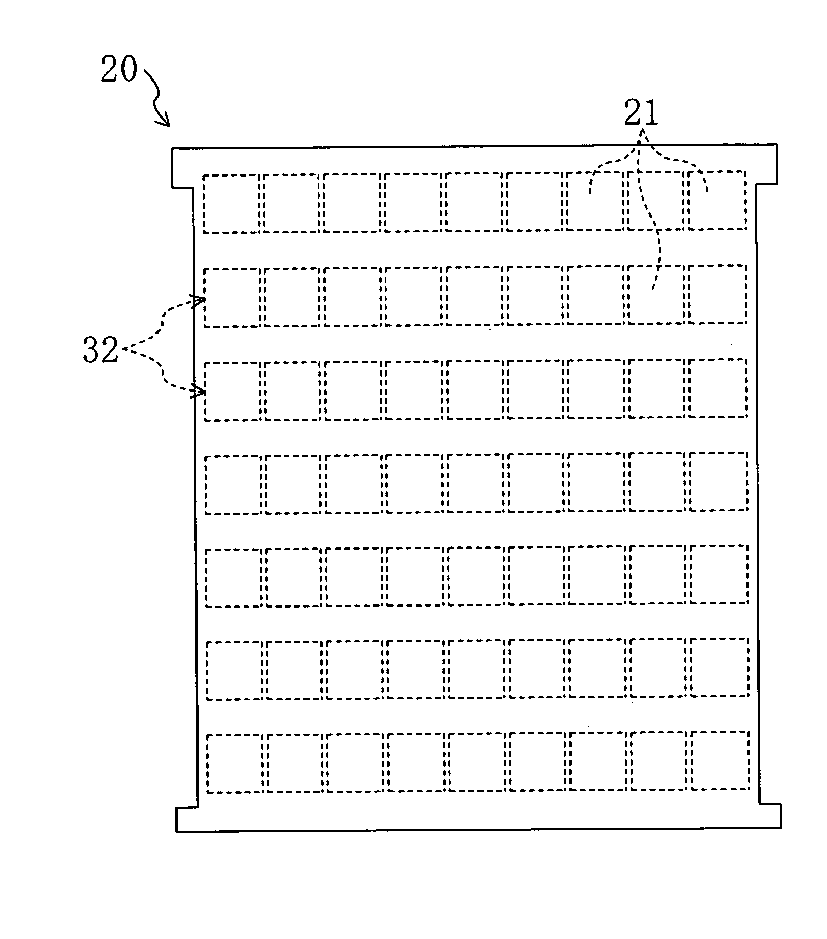
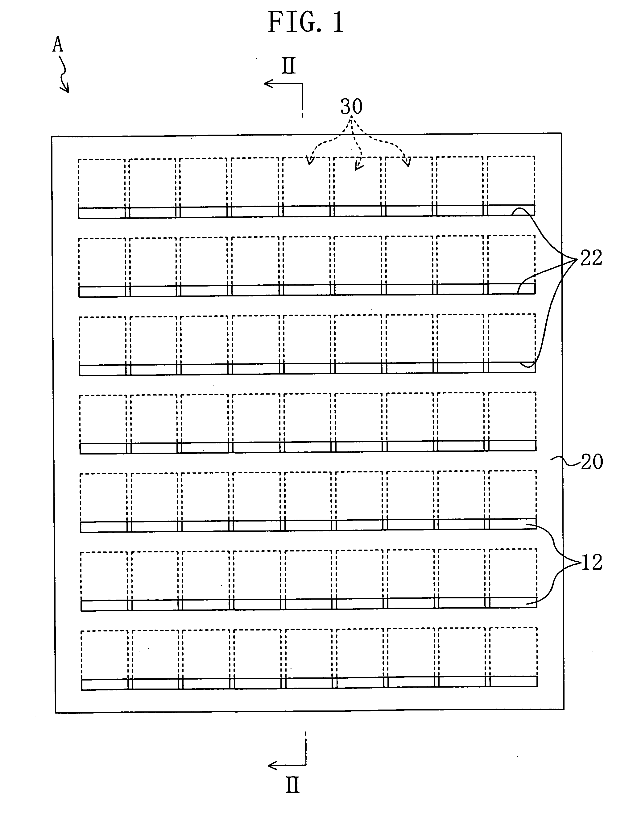
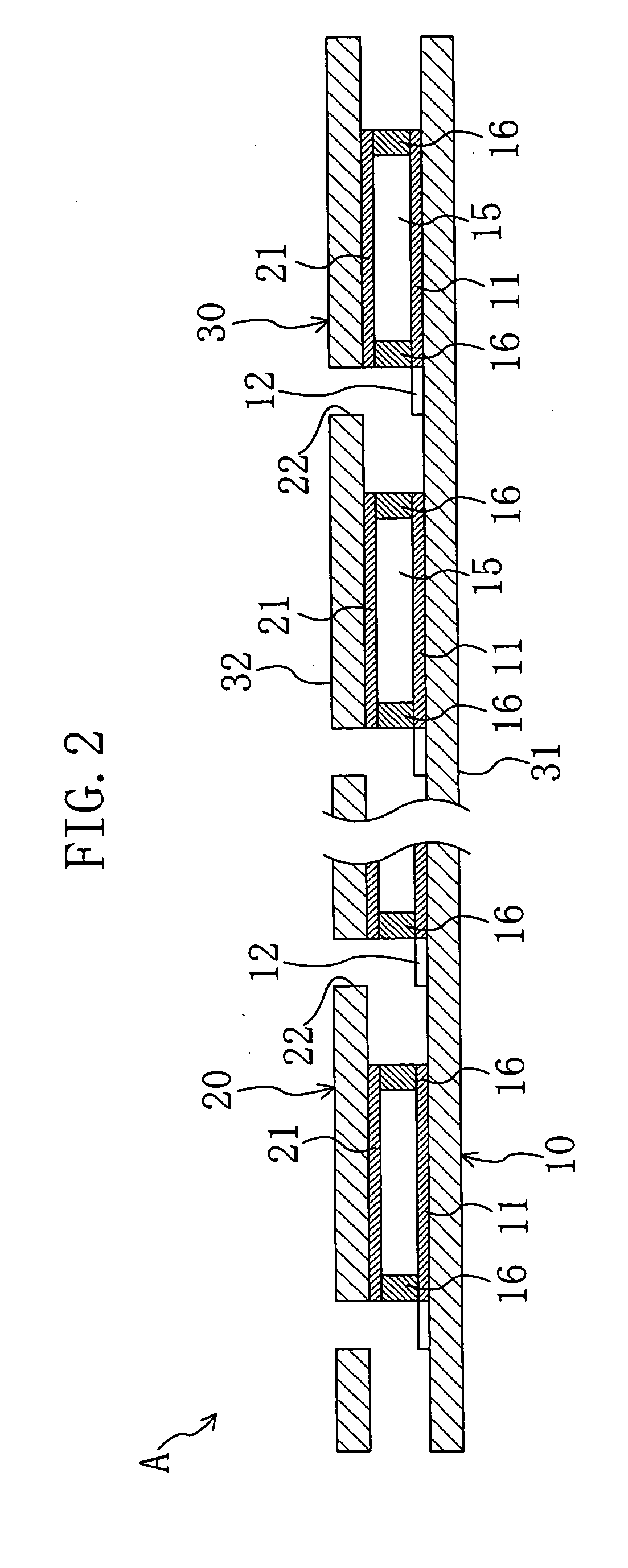
[0051]FIGS. 1 through 4 and FIG. 8 show a liquid crystal panel base material A which is a bonded substrate according to a first embodiment of the invention. FIG. 1 is a front view of the liquid crystal panel base material A according to this embodiment. FIG. 2 is a cross-sectional view schematically showing the liquid crystal panel base material A shown in FIG. 1. FIG. 3 is a front view of a first substrate 10 of the liquid crystal panel base material A according to this embodiment. FIG. 4 is a front view of a second substrate 20 of the liquid crystal panel base material A according to this embodiment. FIG. 8 is a schematic cross-sectional view of a liquid crystal display device S.
[0052]The liquid crystal panel base material A shown in FIGS. 1 and 2 is a base material of liquid crystal display devices S, in which a plurality of liquid crystal panels are integrally arranged in a matrix pattern. In other words, the liquid crystal display devices S are manufactured by dividing the liqu...
second embodiment
[0076]FIGS. 5 through 7 show a liquid crystal panel base material A according to a second embodiment of the invention. Note that, in the embodiments described below, the same portions as those in FIGS. 1 through 4 are denoted by the same reference numerals and detailed description thereof will be omitted. FIG. 5 is a front view of the liquid crystal panel base material A according to this embodiment. FIG. 6 is a diagram showing a first substrate 10 of the liquid crystal panel base material A according to this embodiment. FIG. 7 is a diagram showing a second substrate 20 of the liquid crystal panel base material A according to this embodiment.
[0077]In the first embodiment, the TFT terminal portions 12 are exposed through the openings 22 formed in the second substrate 20. In this embodiment, on the other hand, TFT terminal portions 12 are extended from first electrode layers 11 to a part of a peripheral region of the first substrate 10. The TFT terminal portions 12 are thus exposed fr...
PUM
 Abstract
Description
Claims
Application Information