Printhead Integrated Circuit With More Than Two Metal Layer CMOS

a technology of integrated circuits and metal layers, applied in printing, inking apparatus, etc., can solve the problems of time and cost production efficiency, achieve the effects of reducing the volume of ink, fast refilling time, and limiting the print speed

Inactive Publication Date: 2009-11-05
ZAMTEC +1
View PDF55 Cites 5 Cited by
  • Summary
  • Abstract
  • Description
  • Claims
  • Application Information

AI Technical Summary

Benefits of technology

[0034]Preferably, each of the droplet ejectors has a chamber in which the actuator is positioned, the chamber having a volume less than 30,000 microns cubed. In a further preferred form, the volume is less than 25,000 microns cubed. Low energy ejection of ink droplets generates little, if any, excess heat in the printhead. A build up of excess heat in the printhead imposes a limit on the nozzle firing frequency and thereby limits the print speed. The IJ30 printhead is self cooling (the heat generated by the thermal actuator is removed from the printhead with the ejected drop). In this case, the print speed is only limited by the rate at which the ink can be supplied to the printhead or the speed that the media substrate can be fed past the printhead. Reducing the volume of the ink chambers reduces the volume of ink in which the heat can dissipate. However, a reduced volume ink chamber has a fast refill time and relies solely on capillary action. As the actuator is configured for low energy input, the reduced volume of ink does not cause prob...

Problems solved by technology

Overall, this yields product...

Method used


Image

  • Printhead Integrated Circuit With More Than Two Metal Layer CMOS
  • Printhead Integrated Circuit With More Than Two Metal Layer CMOS
  • Printhead Integrated Circuit With More Than Two Metal Layer CMOS

Examples


Embodiment Construction

[0073]In the preferred embodiment, shape memory materials are utilised to construct an actuator suitable for injecting ink from the nozzle of an ink chamber.

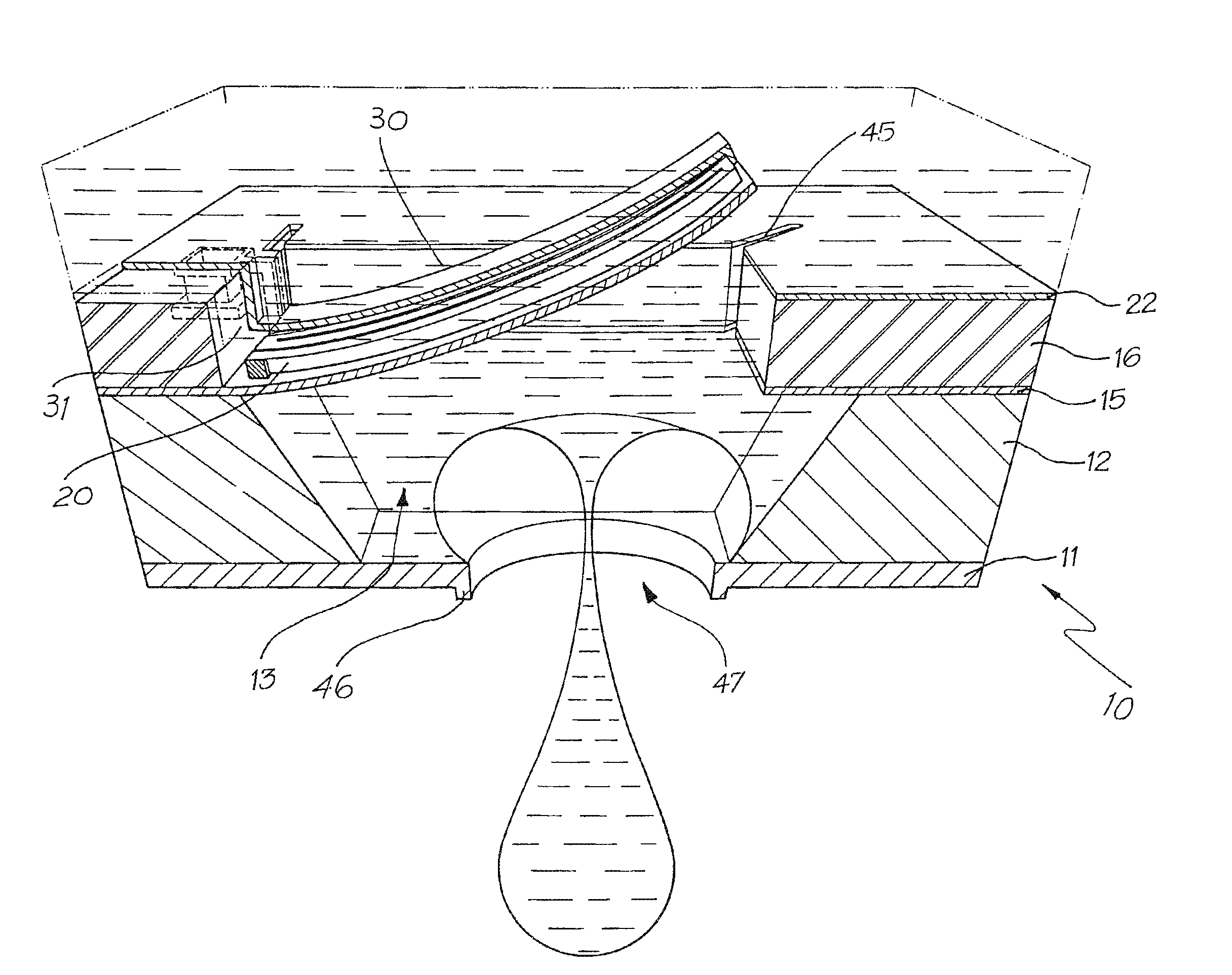
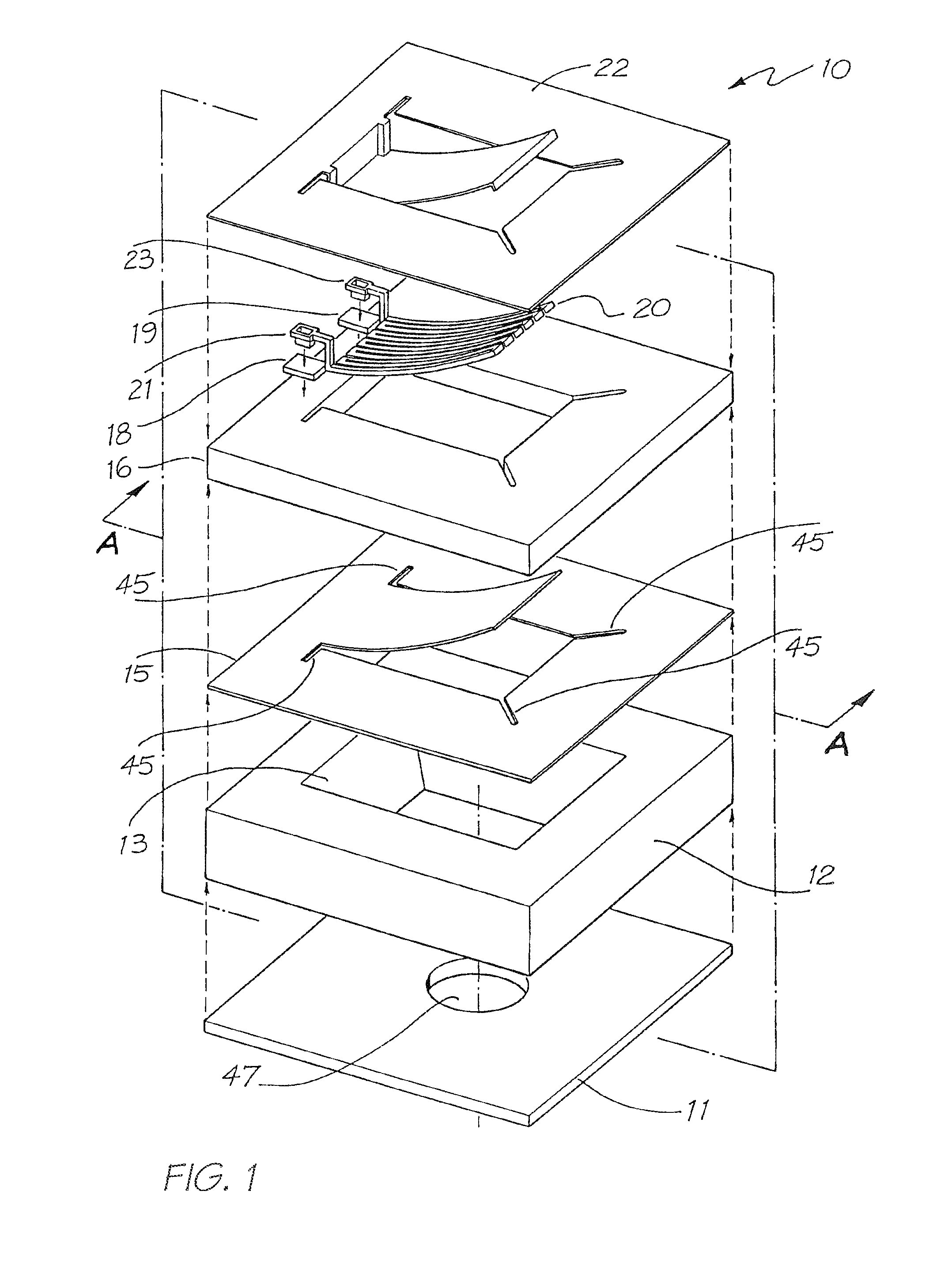
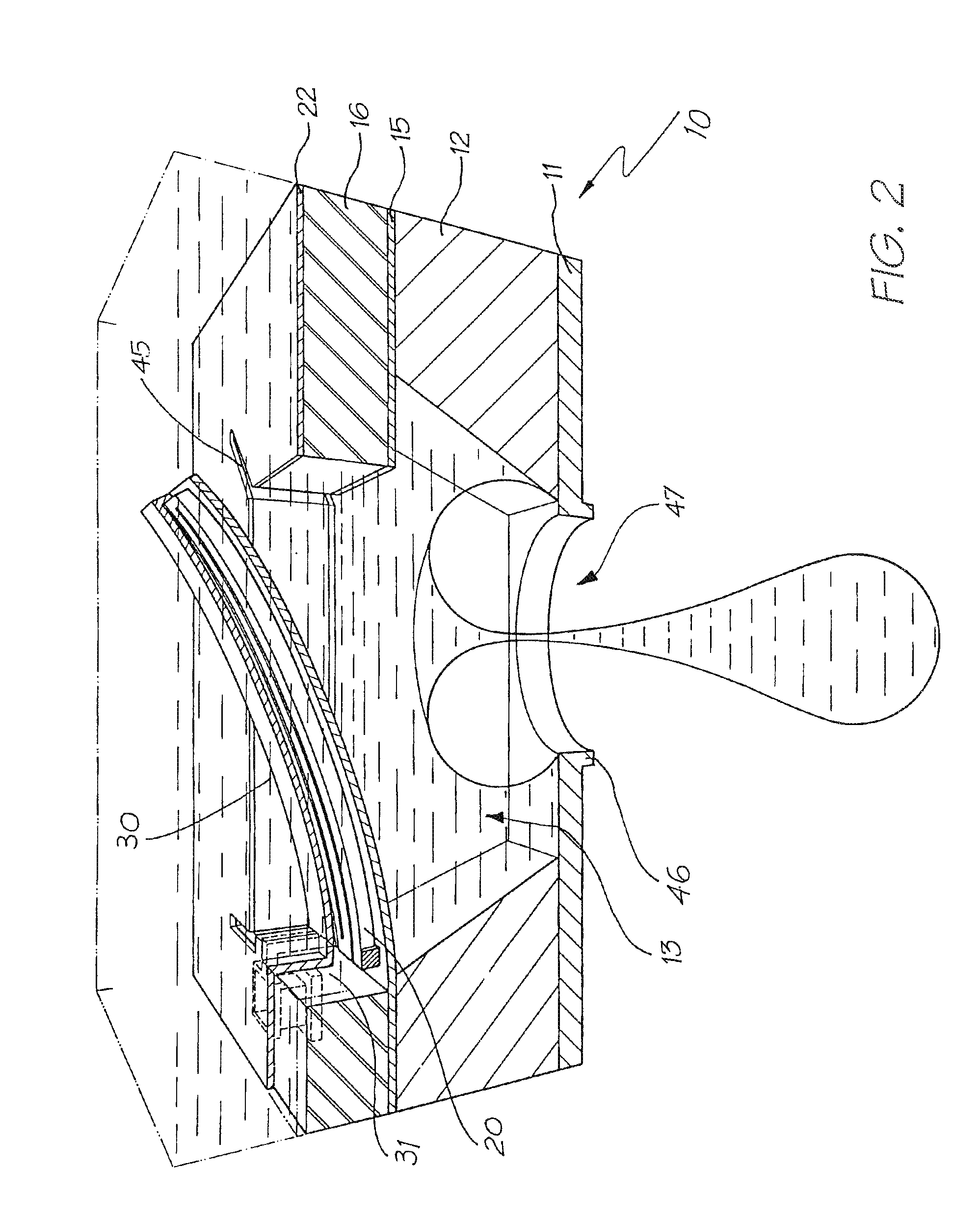
[0074]Turning to FIG. 1, there is illustrated an exploded perspective view 10 of a single ink jet nozzle as constructed in accordance with the preferred embodiment. The ink jet nozzle 10 is constructed from a silicon wafer base utilizing back etching of the wafer to a boron doped epitaxial layer. Hence, the ink jet nozzle 10 comprises a lower layer 11 which is constructed from boron-doped silicon. The boron doped silicon layer is also utilized as a crystallographic etch stop layer. The next layer comprises the silicon layer 12 that includes a crystallographic pit that defines a nozzle chamber 13 having side walls etched at the conventional angle of 54.74 degrees. The layer 12 also includes the various required circuitry and transistors for example, a CMOS layer (not shown). After this, a 0.5-micron thick thermal silicon oxide la...


PUM


Abstract

An inkjet printhead that has an array of droplet ejectors supported on a single printhead integrated circuit (IC). Each of the droplet ejectors has a nozzle aperture and an actuator for ejecting a droplet of ink through the nozzle aperture. The printhead IC also has drive circuitry for providing the actuators with power, the drive circuitry having patterned layers of metal separated by interleaved layers of dielectric material. The layers of metal being interconnected by conductive vias, wherein the drive circuitry has more than two of the metal layers and each of the metal layers are less than 2 microns thick.

Description

CROSS REFERENCE TO RELATED APPLICATIONS[0001]The present application is a continuation-in-part of U.S. application Ser. No. 11 / 926,109 filed on Oct. 28, 2007, which is a continuation of U.S. application Ser. No. 11 / 778,572 filed on Jul. 16, 2007, which is a continuation of U.S. application Ser. No. 11 / 349,074 filed on Feb. 8, 2006, now issued U.S. Pat. No. 7,255,424, which is a continuation of U.S. application Ser. No. 10 / 982,789 filed on Nov. 8, 2004, now issued U.S. Pat. No. 7,086,720, which is a continuation of U.S. application Ser. No. 10 / 421,823 filed on Apr. 24, 2003, now issued U.S. Pat. No. 6,830,316, which is a continuation of U.S. application Ser. No. 09 / 113,122 filed on Jul. 10, 1998, now issued U.S. Pat. No. 6,557,977, all of which are herein incorporated by reference.CROSS REFERENCES TO RELATED APPLICATIONS[0002]The following U.S. patents and U.S. patent applications are hereby incorporated by cross-reference.US Patent / Patent ApplicationIncorporated by Reference:Docket ...

Claims


Application Information

Patent Timeline
IPC IPC(8): B41J2/14
CPCB41J2/14427B41J2/1626B41J2202/03B41J2/1642B41J2/1648B41J2/1631
Inventor SILVERBROOK, KIA
Owner ZAMTEC
Why Eureka
Try Eureka