Optical semiconductor module, adjusting method thereof, and fabricating method thereof

a technology of optical semiconductor modules and manufacturing methods, which is applied in the direction of semiconductor lasers, instruments, optical elements, etc., can solve the problems of inability to install optical isolators exclusively, inability to achieve the installation of optical isolators, and possible over-exceeding of laser beam output intensity, etc., so as to reduce production costs and suppress variations of characteristics.

Inactive Publication Date: 2009-11-05
NEC ELECTRONICS CORP
View PDF1 Cites 13 Cited by
  • Summary
  • Abstract
  • Description
  • Claims
  • Application Information

AI Technical Summary

Benefits of technology

[0018]The semiconductor laser, the lens and the optical connector are aligned such that the spot diameter of the laser beam on the incident plane becomes smaller than the diameter of the core of the optical fiber. That is, the defocusing quantity falls within a range in which the coupling efficiency is kept maximum, and therefore, no laser beam can be attenuated caused by the defocusing. In this case, the diameter of the core of the optical fiber to be inserted into the optical connector becomes irrelevant. The optical output of the light propagating through the optical fiber becomes almost constant irrespective of the SMF or the MMF to be inserted into the optical connector. Consequently, variations of the characteristics can be suppressed in the system in which an arbitrary optical fiber is inserted into the optical connector. In this manner, according to the present invention, it is possible to achieve the optical semiconductor module having a constant output irrespective of the type of optical fiber to be inserted.
[0019]According to the present invention, the output of optical semiconductor module can be constantly kept irrespective of the type of optical fiber to be inserted. Additionally, since no optical isolator is used for adjusting the amount of light, production cost can be reduced.

Problems solved by technology

An optical isolator is often used in a distributed feed-back (abbreviated as “DFB”) laser which is relatively liable to undergo an influence of a reflecting return light, and further, is very expensive.
Therefore, it is not practical to dare to install an optical isolator exclusively for the adjustment of the light amount in an optical semiconductor module which does not usually require any optical isolator.
However, in this case, the output intensity of the laser beam may possibly exceed a desired output intensity.

Method used


Image

  • Optical semiconductor module, adjusting method thereof, and fabricating method thereof
  • Optical semiconductor module, adjusting method thereof, and fabricating method thereof
  • Optical semiconductor module, adjusting method thereof, and fabricating method thereof

Examples


Embodiment Construction

[0027]The invention will be now described herein with reference to illustrative embodiments. Those skilled in the art will recognize that many alternative embodiments can be accomplished using the teachings of the present invention and that the invention is not limited to the embodiments illustrated for explanatory purposed.

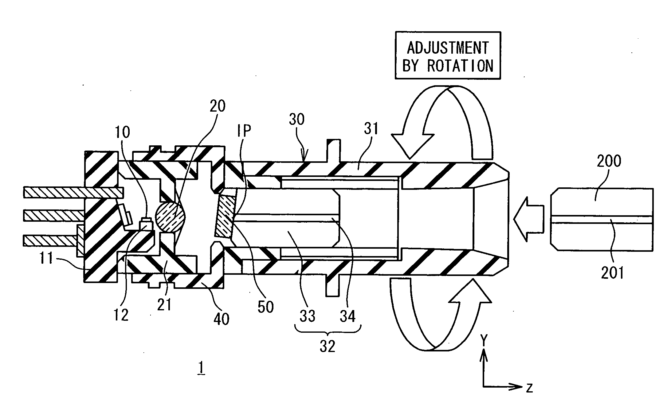
[0028]FIG. 4 is a cross-sectional view schematically showing a configuration of an optical semiconductor module 1 according to an embodiment of the present invention. The optical semiconductor module 1 is provided with a semiconductor laser 10, an optical lens 20, and a receptacle 30.

[0029]The semiconductor laser 10 is a laser diode for radiating a laser beam. In particular, it is preferable that the semiconductor laser 10 is a Fabry-Perot laser diode. The semiconductor laser 10 is mounted on a sub-mount 12 joined to a stem 11 by soldering or the like. The optical lens20 converges the laser beam radiated from the semiconductor laser 10. The optical lens 20 is fix...


PUM


Abstract

An optical semiconductor module has: a semiconductor laser for radiating a laser beam; a lens for converging the laser beam; and an optical connector outputting the laser beam received from the lens to a transmission path. The optical connector has: a fiber ferrule including an optical fiber with an incident plane of the laser beam; and a light attenuator covering the incident plane. Transmittance of the laser beam through the light attenuator is varied according to rotation of the light attenuator on a plane perpendicular to an optical axis. The semiconductor laser, the lens and the optical connector are aligned such that a spot diameter of the laser beam on the incident plane is smaller than a diameter of a core of the optical fiber.

Description

BACKGROUND OF THE INVENTION[0001]1. Field of the Invention[0002]The present invention relates to an optical semiconductor module. In particular, the present invention relates to a technique for adjusting an output of an optical semiconductor module.[0003]2. Description of the Related Art[0004]There has been known an “optical semiconductor module” for use in transmitting light in the field of optical communications (see, for example, Japanese Laid-Open Patent Application JP-2004-205861, Japanese Laid-Open Patent Application JP-2004-138864 and Japanese Laid-Open Patent Application JP-H09-307144). The optical semiconductor module includes a semiconductor laser (a laser diode) serving as a light emitting device, and an optical connector for holding therein an optical fiber, wherein the semiconductor laser and the optical fiber are optically coupled to each other. For example, in a case where a receptacle is used as the optical connector, the optical semiconductor module is referred to a...

Claims


Application Information

Patent Timeline
Patent Type & Authority Applications(United States)
IPC IPC(8): G02B6/36
CPCG02B6/266G02B6/4204G02B6/421H01S5/02296H01S5/005H01S5/02212H01S5/02284G02B6/4292H01S5/02251H01S5/02257
Inventor ARAYAMA, TATSUROUKURIHARA, YUSUKE
Owner NEC ELECTRONICS CORP
Why Eureka
Try Eureka