Methods of removing silicon oxide and gaseous mixtures for achieving same

a gaseous mixture and silicon oxide technology, applied in the direction of decorative surface effects, electrical appliances, decorative arts, etc., can solve the problems of reducing the wafer throughput and adding time to the wafer fabrication process

Active Publication Date: 2009-11-05
MICRON TECH INC
View PDF34 Cites 630 Cited by
  • Summary
  • Abstract
  • Description
  • Claims
  • Application Information

AI Technical Summary

Problems solved by technology

Semiconductor wafers undergoing the COR / PHT process are transported from one chamber to the other, which adds time to the wafer fabrication process and decreases wafer throughput.

Method used


Image

  • Methods of removing silicon oxide and gaseous mixtures for achieving same
  • Methods of removing silicon oxide and gaseous mixtures for achieving same
  • Methods of removing silicon oxide and gaseous mixtures for achieving same

Examples


Embodiment Construction

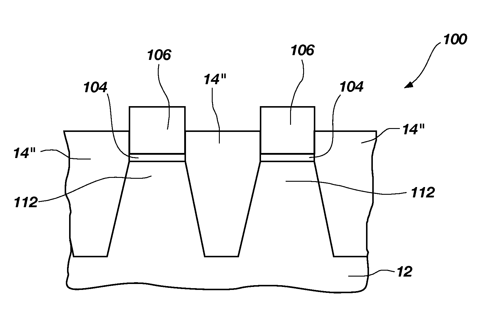
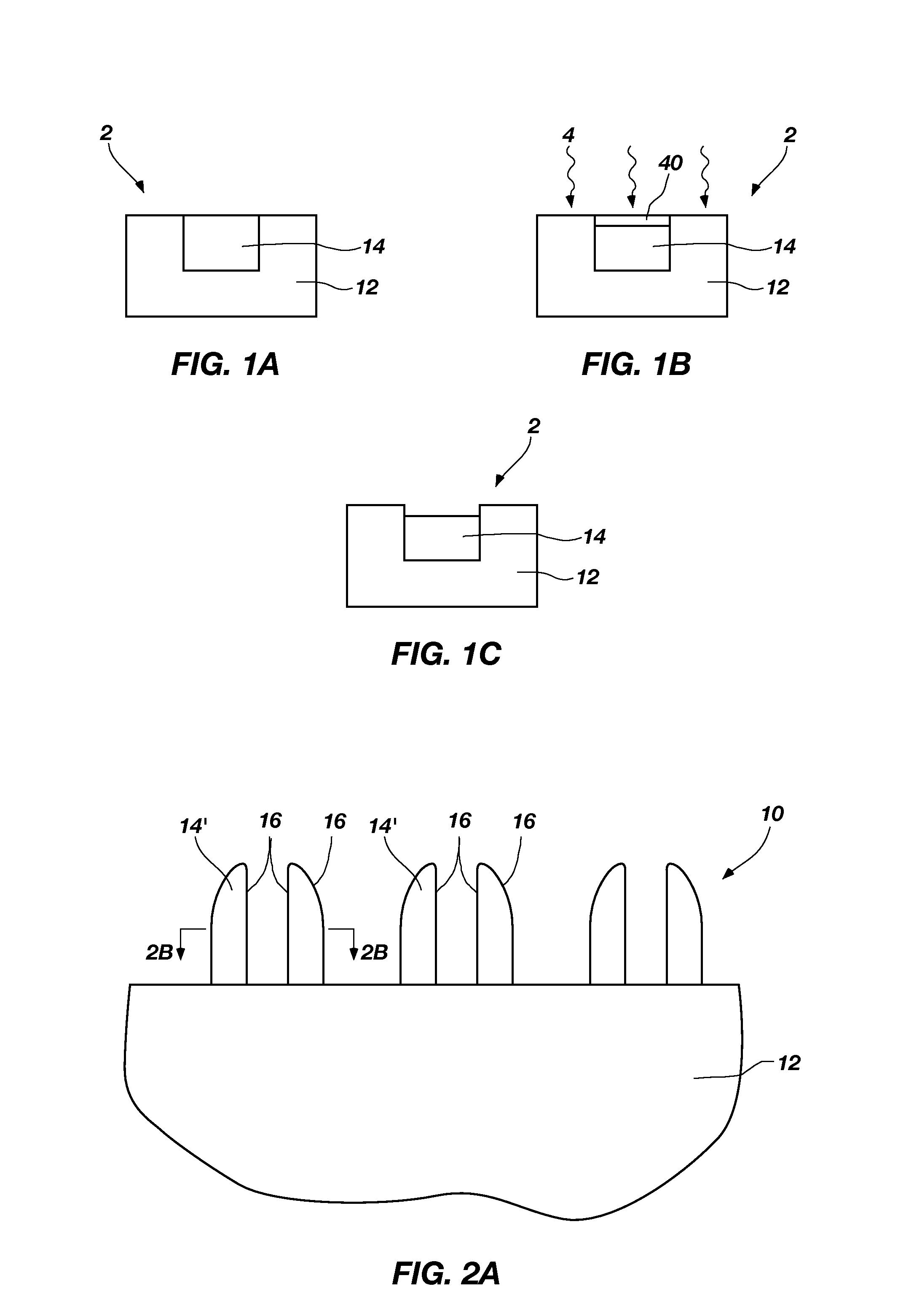
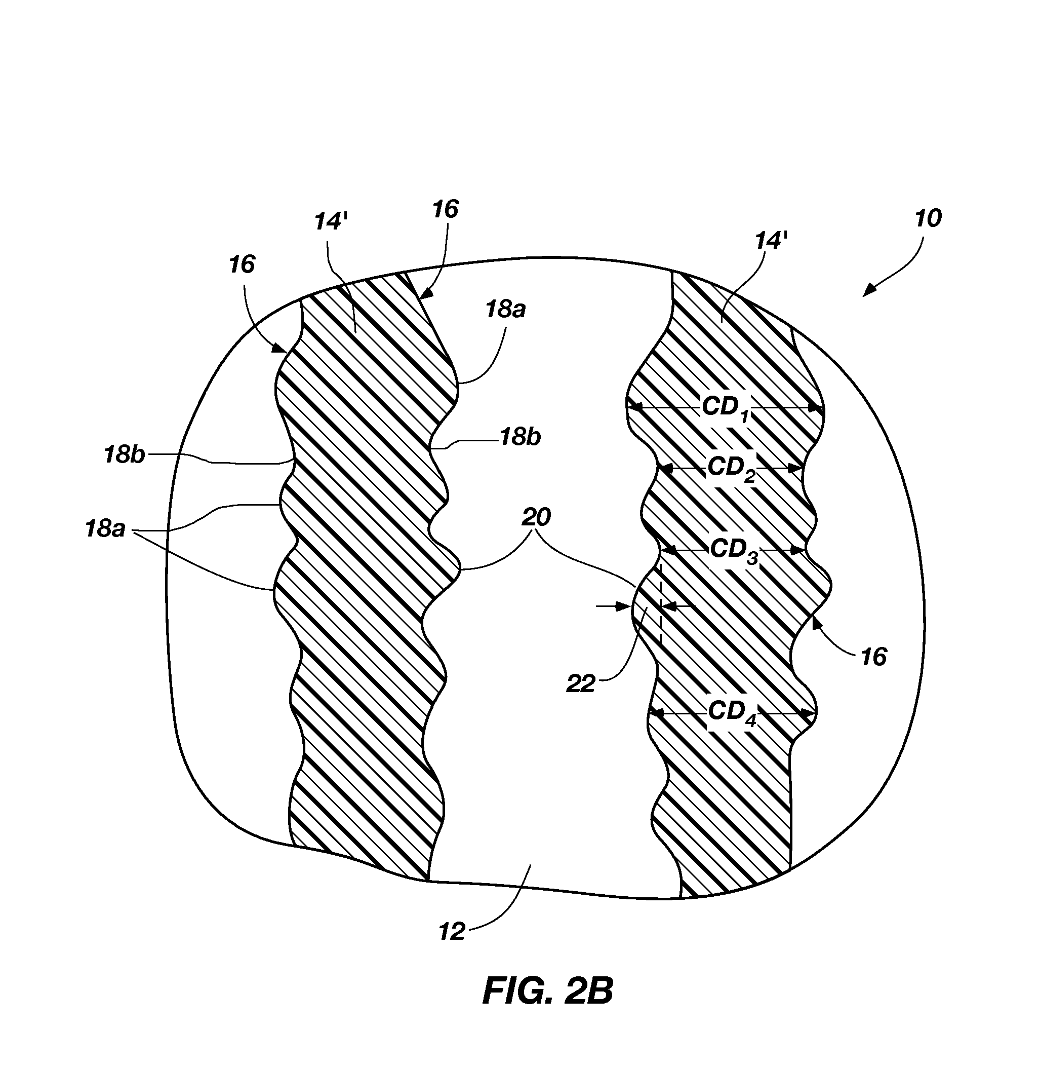
[0011]A method of removing at least a portion of a silicon oxide material is disclosed. As shown in FIGS. 1A-1C, a semiconductor structure 2 including a substrate 12 and a silicon oxide 14 (“SiOx”) is provided. A surface of the silicon oxide 14 is exposed to an ammonium fluoride chemistry, forming a solid reaction product 40 on the surface of the silicon oxide 14. As described in more detail below, the ammonium fluoride chemistry includes a volatile amine and HF. The reaction of the volatile amine and HF with the silicon oxide 14 is referred to herein as “ammonium fluoride chemical treatment” to distinguish this reaction from the chemical treatment of the conventional COR / PHT process. The solid reaction product 40 and silicon oxide 14 are exposed to a plasma 4, producing volatile species that are easily removed from a processing chamber (not shown) in which the plasma 4 is produced. Subjecting the silicon oxide 14 and the solid reaction product 40 to the plasma 4 is referred to here...


PUM

PropertyMeasurementUnit
ion bombardment energyaaaaaaaaaa
temperatureaaaaaaaaaa

Abstract

A method of removing at least a portion of a silicon oxide material is disclosed. The silicon oxide is removed by exposing a semiconductor structure comprising a substrate and the silicon oxide to an ammonium fluoride chemical treatment and a subsequent plasma treatment, both of which may be effected in the same vacuum chamber of a processing apparatus. The ammonium fluoride chemical treatment converts the silicon oxide to a solid reaction product in a self-limiting reaction, the solid reaction product then being volatilized by the plasma treatment. The plasma treatment includes a plasma having an ion bombardment energy of less than or equal to approximately 20 eV. An ammonium fluoride chemical treatment including an alkylated ammonia derivative and hydrogen fluoride is also disclosed.

Description

TECHNICAL FIELD[0001]Embodiments of the invention relate to fabricating semiconductor structures and, more specifically, to removing silicon oxide from semiconductor structures.BACKGROUND[0002]Chemical Oxide Removal (“COR”) is a gaseous process known in the art to selectively remove silicon oxides (“SiOx”) by reacting gaseous ammonia (“NH3”) and hydrogen fluoride (“HF”) to produce NH4Fx. The NH3 and HF react with silicon oxide on a semiconductor wafer to form ammonium hexafluorosilicate (“(NH4)2SiF6”). This reaction is referred to herein as a “chemical treatment” and is typically conducted in a reaction chamber. The semiconductor wafer is then transferred to a different chamber and heated, producing nitrogen (“N2”), water (“H2O”), silicon tetrafluoride (“SiF4”), and NH3, which are volatile and evaporate from the surface of the semiconductor wafer. Heating the semiconductor wafer is referred to herein as a “post heat treatment (“PHT”).” Alternatively, the (NH4)2SiF6 is removed using ...

Claims


Application Information

Patent Timeline
Patent Type & Authority Applications(United States)
IPC IPC(8): H01L21/302
CPCH01L21/31116H01L21/0337
Inventor KIEHLBAUCH, MARK W.GREELEY, J. NEILMORGAN, PAUL A.
Owner MICRON TECH INC
Why Eureka
Try Eureka