Lithographic apparatus and device manufacturing method

a technology of lithographic apparatus and manufacturing method, which is applied in the direction of printers, instruments, optical radiation measurement, etc., can solve the problems of inconvenient large-scale manufacture of devices with acceptable throughput and design of photolithographic apparatus, and achieves reliable, leak-free connection and simple manufacturing. , the effect of simplifying the connection to the chamber

Active Publication Date: 2008-04-15
ASML NETHERLANDS BV
View PDF82 Cites 92 Cited by
  • Summary
  • Abstract
  • Description
  • Claims
  • Application Information

AI Technical Summary

Benefits of technology

[0012]In an exemplary embodiment of the invention, the fluid processing cell includes a plate member having walls projecting therefrom to contact the substrate to define the plurality of chambers. Such a construction is simple to manufacture and allows the separate chambers to be spaced as close as possible together. The plate member can be integrated into the substrate table, e.g. forming a pimple table, or placed on the substrate on the

Problems solved by technology

Existing photolithographic apparatus designeded for advanced semiconductor manufacture or manufacture on large area substrates, e.g for flat panel displays, ar

Method used


Image

  • Lithographic apparatus and device manufacturing method
  • Lithographic apparatus and device manufacturing method
  • Lithographic apparatus and device manufacturing method

Examples


third embodiment

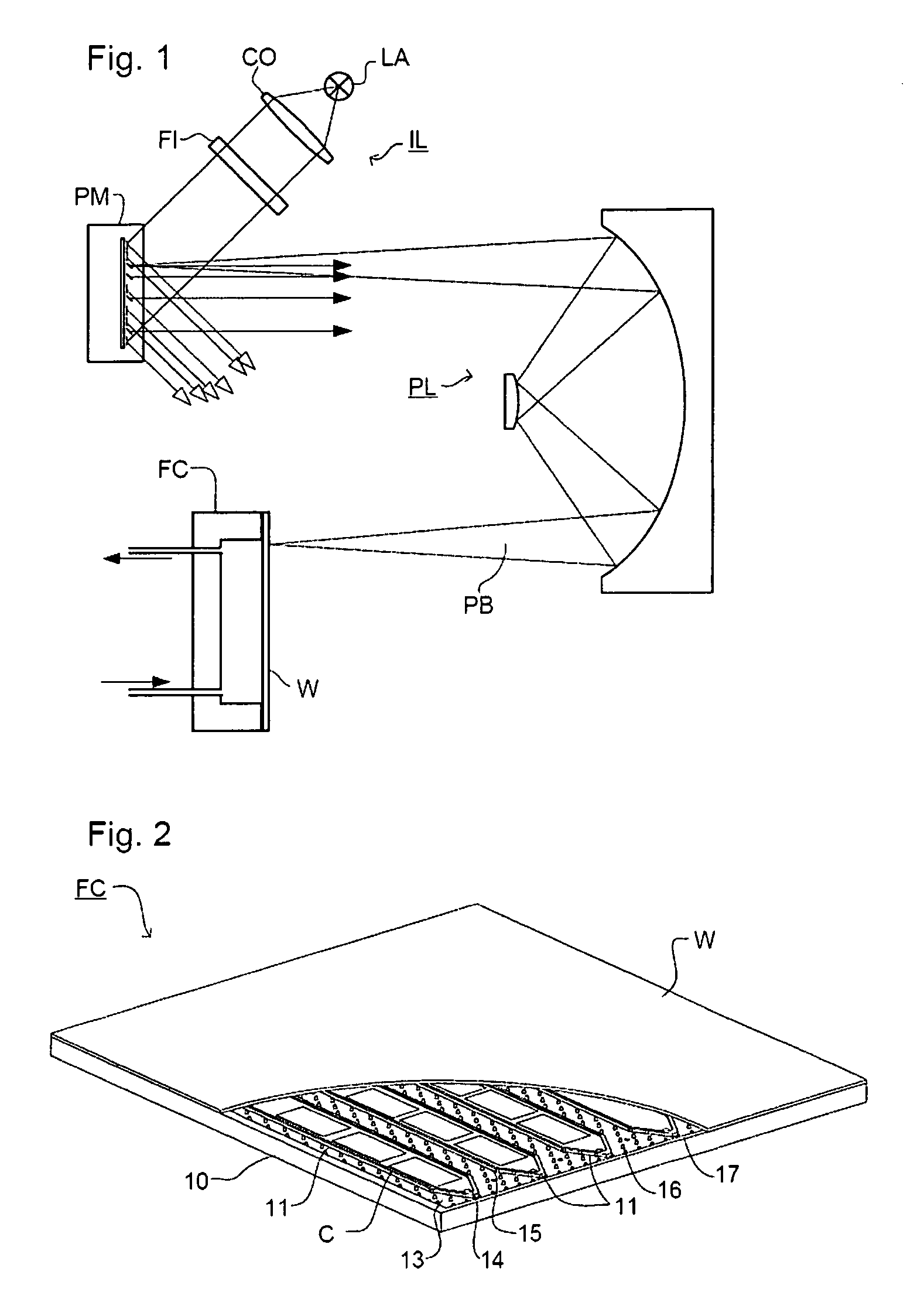
[0065]In the third embodiment, the substrate table WT is provided with a well 78 which is deep enough to accommodate the thickest substrates expected, e.g. substrates bonded to carriers. When a thinner substrate is to be used, a dummy or spacer substrate 79 of appropriate thickness to bring the top surface of the substrate W to the correct height is employed.

[0066]A fourth embodiment of the invention is shown in FIG. 9 and is again a variant of the second embodiment. Parts similar to those of the second embodiment are denoted by references 20 higher.

fourth embodiment

[0067]The fourth embodiment omits the peripheral walls 63 for simplicity and to accommodate variation in the substrate thickness. The fluid is allowed to flow over the edge of the substrate so if a pimple table and vacuum arrangement is used to hold the substrate in place, the vacuum system must be able to accept any leakage of fluid under the substrate that may occur.


PUM

PropertyMeasurementUnit
Areaaaaaaaaaaa
Heightaaaaaaaaaa
Sensitivityaaaaaaaaaa

Abstract

A flowcell including a plurality of separate chambers is provided on the substrate table so that a fluid can be brought into contact with exposed areas of the substrate to interact therewith. A series of exposures and chemical processes can thereby be carried out without removing the substrate from the substrate table.

Description

BACKGROUND OF THE APPLICATION[0001]This application claims priority to EP02258278.7, filed Nov. 29, 2002, the entire contents of which is incorporated herein by reference.BACKGROUND OF THE INVENTION[0002]1. Field of the Invention[0003]The present invention relates to a lithographic apparatus, particularly to such apparatus adapted to manufacture so-called “bio-chips”, and a device manufacturing method.[0004]2. Description of the Related Art[0005]A lithographic apparatus is a machine that applies a desired pattern onto a target portion of a substrate. Lithographic apparatus can be used, for example, in the manufacture of integrated circuits (ICs). In that circumstance, a patterning structure, such as a mask, may be used to generate a circuit pattern corresponding to an individual layer of the IC, and this pattern can be imaged onto a target portion (e.g comprising part of, one or several dies) on a substrate (e.g. a silicon wafer) that has a layer of radiation-sensitive material (res...

Claims


Application Information

Patent Timeline
IPC IPC(8): G03B27/42G03B27/58B81C1/00C40B60/14G03F7/20
CPCG03F7/708B82Y30/00B01J2219/00353B01J2219/00432B01J2219/00434B01J2219/00439B01J2219/00711B01J2219/0072C40B60/14B01J2219/00448G03F7/20
Inventor SIMON, KLAUSLOF, JOERIMINNAERT, ARTHUR WINFRIED EDUARDUSSMEETS, ERIK MARIE JOSE
Owner ASML NETHERLANDS BV
Why Eureka
Try Eureka