Touch panel and input device using same

a technology of input device and touch panel, which is applied in the field of touch panel, can solve the problems of inability to meet the electrical contact between the upper conductive layer and the cost of materials and processing for manufacturing the touch panel, and achieve the effects of low elasticity, low cost, and low cos

Inactive Publication Date: 2009-11-19
PANASONIC CORP
View PDF7 Cites 45 Cited by
  • Summary
  • Abstract
  • Description
  • Claims
  • Application Information

AI Technical Summary

Benefits of technology

[0016]Since the decorative sheet is formed thinner than that of a conventional frame window section, it can virtually eliminate a difference in level throughout an operating area on the upper surface when the touch panel is attached to the front face of an input device. The present invention can thus provide the touch panel featuring high stability in making electrical contact in the end use without requiring any special material having a low elasticity to form the spacer.

Problems solved by technology

When such practice is repeated, a large force exerted upon these areas of top substrate 1 and upper conductive layer 3 causes cracks and fractures in upper conductive layer 3 on the lower surface of top substrate 1, which can lead to instability in the electrical contact between upper conductive layer 3 and lower conductive layer 4.
The above structure still has a problem, however, that materials suitable for spacer 8 are limited, and costs of the materials and processing for manufacturing the touch panel became rather expensive.

Method used


Image

  • Touch panel and input device using same
  • Touch panel and input device using same
  • Touch panel and input device using same

Examples


Embodiment Construction

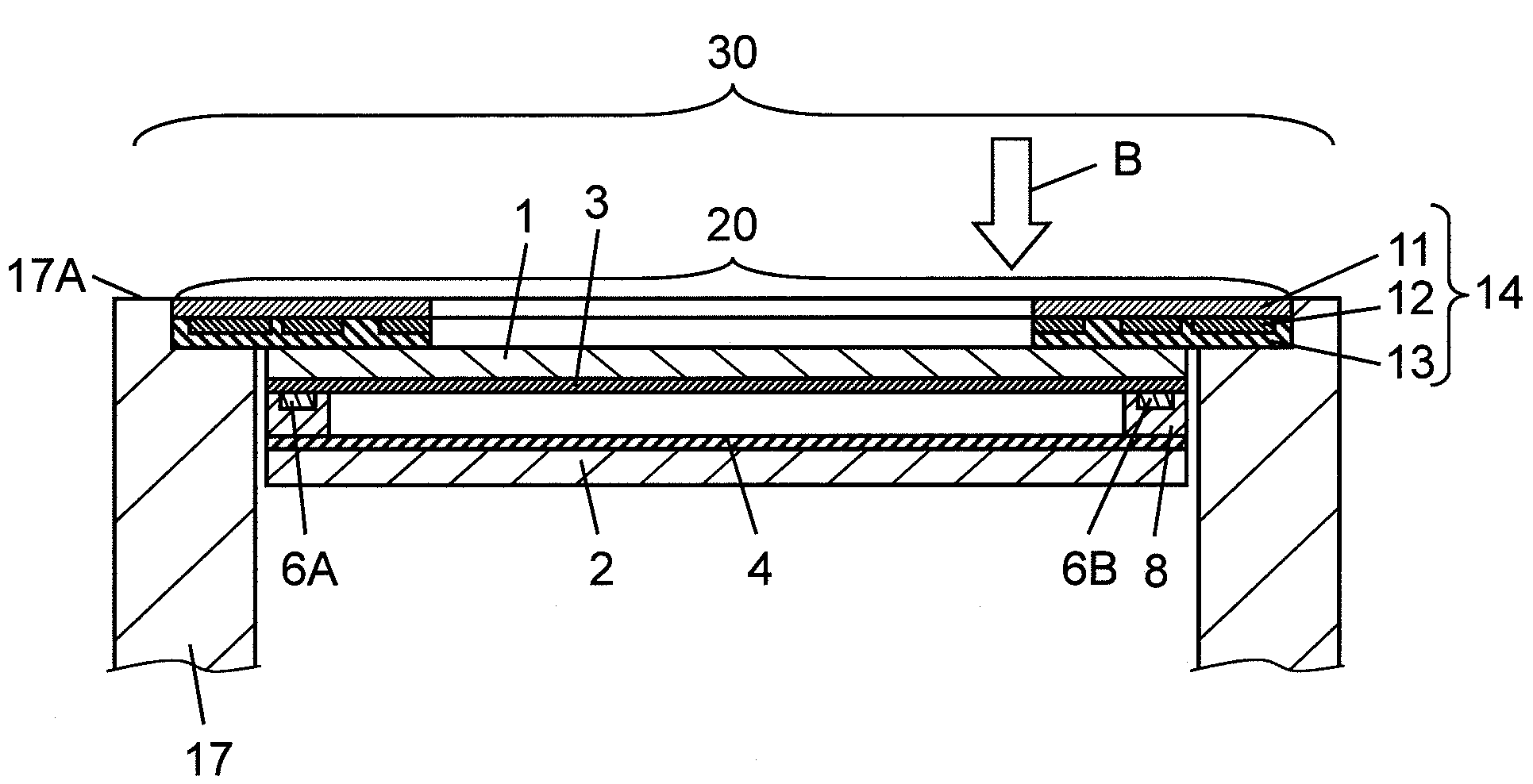
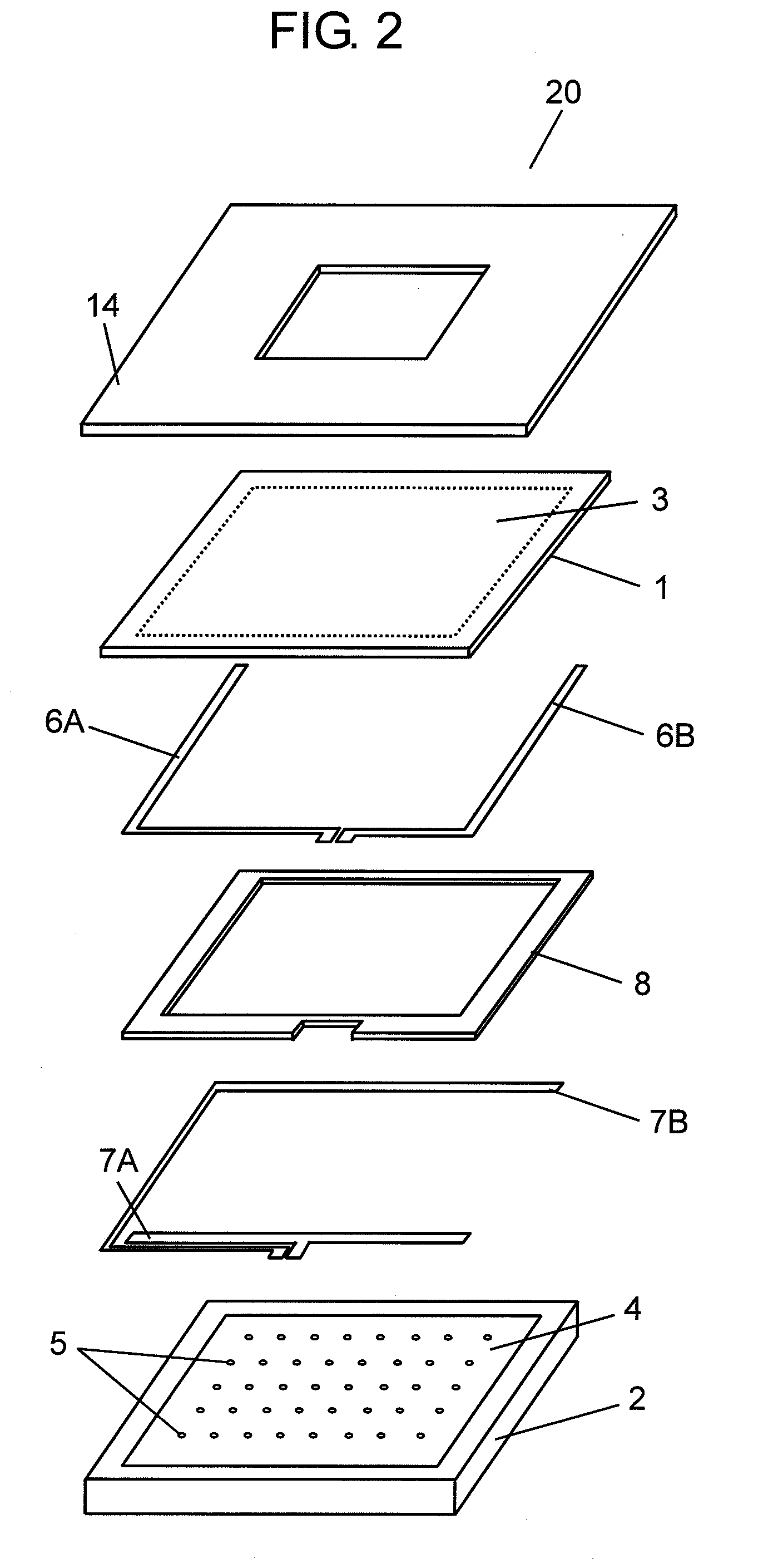
[0024]Description is provided hereinafter of exemplary embodiments of the present invention with reference to FIG. 1 through FIG. 6.

[0025]The sectional views shown in these figures are enlarged in the direction of thickness to help understand the structures easily.

[0026]In addition, like reference marks are used throughout to designate like structural components as those illustrated in the background art, and their descriptions will be abbreviated.

Exemplary Embodiments

[0027]FIG. 1 is a sectional view of a touch panel according to one exemplary embodiment of the present invention, and FIG. 2 is an exploded perspective view of the touch panel. In FIGS. 1 and 2, top substrate 1 is an optically transparent substrate of a material such as polyether sulfone, polycarbonate, glass and the like. Bottom substrate 2 is also an optically transparent substrate of a material such as glass, acrylic, polycarbonate and the like. Top substrate 1 is provided with optically transparent upper conductive...


PUM


Abstract

A touch panel including a top substrate provided with an upper conductive layer formed on a lower surface thereof, a bottom substrate provided with a lower conductive layer formed on an upper surface thereof in a position confronting the upper conductive layer with a predetermined space, and a spacer of a frame-like shape formed at a periphery of at least one of the top substrate and the bottom substrate, and formed therebetween, wherein the touch panel further has a decorative sheet disposed on an upper surface of the top substrate so that a peripheral edge of the decorative sheet protrudes outward beyond the periphery of the top substrate.

Description

FIELD OF THE INVENTION[0001]The present invention relates to touch panels used mainly for operating a variety of input devices, and also to input devices using the same.BACKGROUND OF THE INVENTION[0002]With the advancement in recent years toward greater functionality and versatility of input devices of various types for use in mobile phones, car navigation systems and the like, many apparatuses are now equipped with optically transparent touch panels mounted to front plates of display devices such as liquid crystal displays. On the growing use is a type of input devices that allow users to press touch panels with a finger, a pen or the like medium to select any of functions on the input devices while visually checking screens on the display devices located behind the see-through touch panels.[0003]Japanese Patent Unexamined Publication, No. 2003-280800, for instance, discloses a conventional touch panel of such type, description of which is now provided with reference to FIG. 7. The...

Claims


Application Information

Patent Timeline
Patent Type & Authority Applications(United States)
IPC IPC(8): G06F3/041
CPCG06F3/045
Inventor NAKANISHI, AKIRAFUJII, SHIGEYUKI
Owner PANASONIC CORP
Why Eureka
Try Eureka