Nonvolatile storage device and method for manufacturing same

a storage device and non-volatile technology, applied in semiconductor devices, digital storage, instruments, etc., can solve the problems of limiting the improvement of its characteristics, reliability, operating speed, bit density, etc., and achieve the effect of improving the uniformity of characteristics, reliability, and operation speed

Inactive Publication Date: 2009-12-03
KK TOSHIBA
View PDF5 Cites 29 Cited by
  • Summary
  • Abstract
  • Description
  • Claims
  • Application Information

AI Technical Summary

Problems solved by technology

However, a NAND flash memory is based on the operation of a transistor which records information using its threshold voltage variation, and reportedly has limitations on further improvement of its characteristics uniformity, reliability, operating speed, and bit density.

Method used


Image

  • Nonvolatile storage device and method for manufacturing same
  • Nonvolatile storage device and method for manufacturing same
  • Nonvolatile storage device and method for manufacturing same

Examples


example 1

PRACTICAL EXAMPLE 1

[0113]Next, a first practical example (Practical example 1) of the nonvolatile storage device according to this embodiment is described with reference to FIGS. 9A to 13.

[0114]First, the nonvolatile storage device according to Practical example 1 is described with reference to FIG. 13.

[0115]FIG. 13 is a schematic perspective view illustrating the configuration of a nonvolatile storage device 2P according to Practical example 1 (this is also a schematic process perspective view as described later).

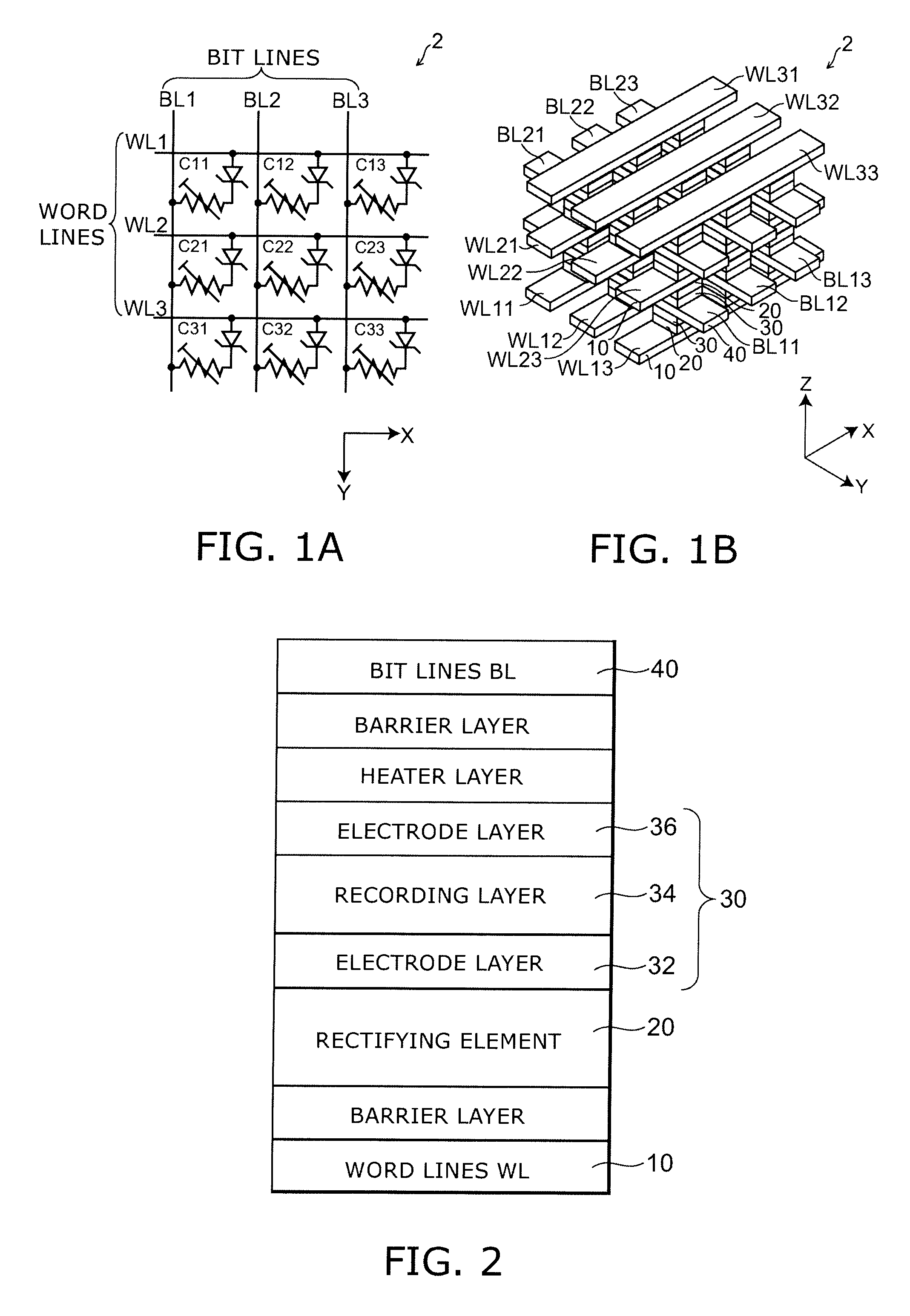
[0116]The nonvolatile storage device 2P according to Practical example 1 has a structure similar to that of the nonvolatile storage device 2 according to Example 1, except that the bit lines and the word lines are interchanged in FIGS. 1A and 1B. More specifically, in the configuration of FIGS. 1A and 1B, sequentially from bottom, bit lines, word lines, bit lines, word lines, and bit lines are arranged. Furthermore, in the configuration illustrated in FIG. 2, one unit memo...

example 2

PRACTICAL EXAMPLE 2

[0148]Next, a second practical example (Practical example 2) of the nonvolatile storage device according to this embodiment is described with reference to FIGS. 14 to 18B.

[0149]First, the nonvolatile storage device according to Practical example 2 is described with reference to FIG. 14.

[0150]FIG. 14 is a schematic perspective view illustrating the configuration of a nonvolatile storage device 2Q according to Practical example 2. For clarity of illustration of the multilayer structure, interlayer dielectric films are not shown.

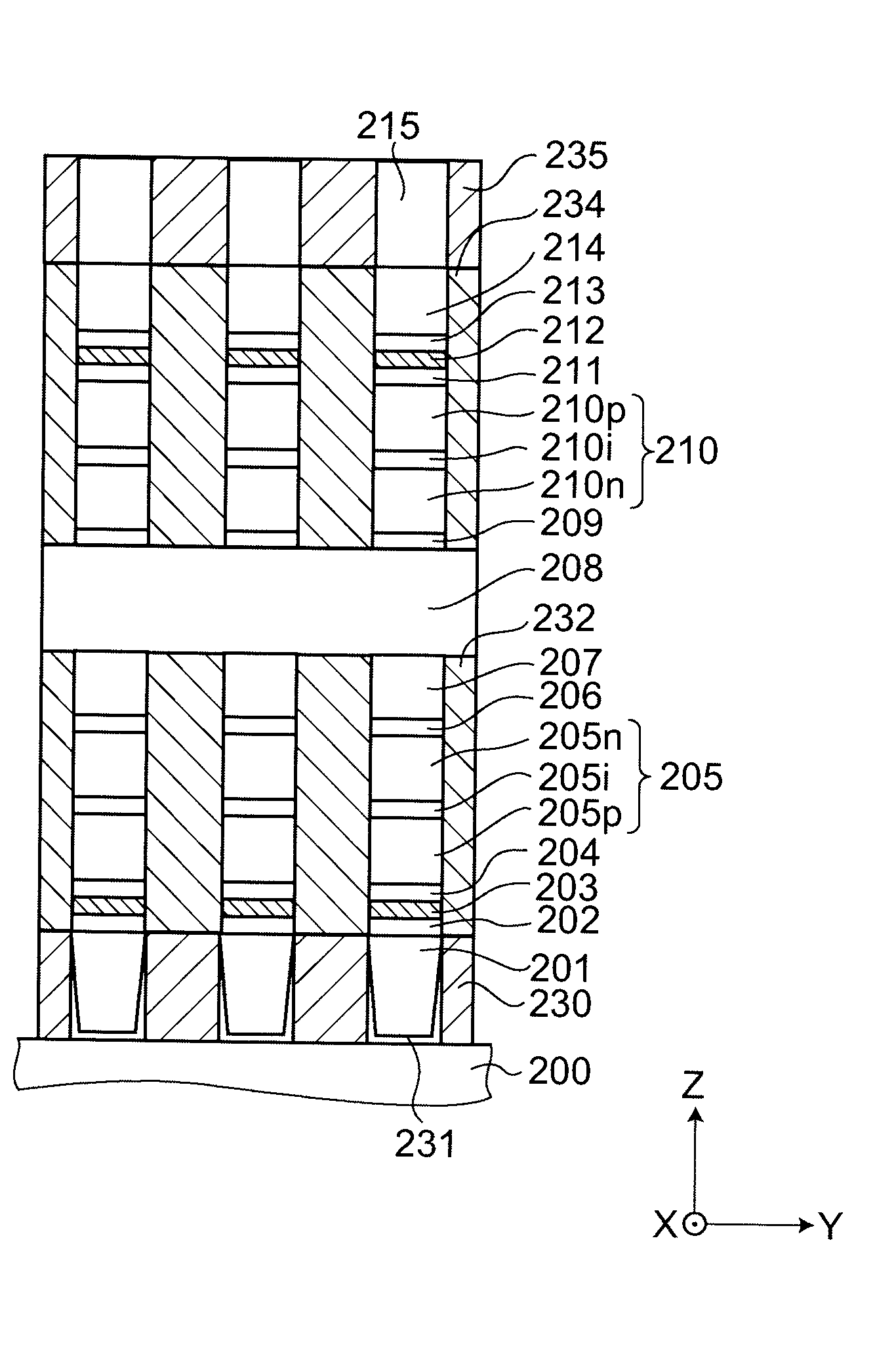
[0151]As shown in FIG. 14, the nonvolatile storage device 2Q according to Practical example 2 has a structure similar to that of the nonvolatile storage device 2P according to Practical example 1. More specifically, as shown, bit lines 201, an electrode layer 202, a recording layer 203, an electrode layer 204, a rectifying element 205, word lines 208, a rectifying element 210, an electrode layer 211, a recording layer 212, an electrode layer ...


PUM


Abstract

A method for manufacturing a nonvolatile storage device with a plurality of unit memory layers stacked therein is provided. Each of the unit memory layers includes: a first interconnect extending in a first direction; a second interconnect extending in a second direction; a recording unit sandwiched between the first and second interconnects and being capable of reversibly transitioning between a first state and a second state in response to a current supplied through the first and second interconnects; and a rectifying element sandwiched between the first interconnect and the recording unit and including at least one of p-type and n-type impurities. In the method, the first interconnect, the second interconnect, the recording unit, and a layer of an amorphous material including the at least one of p-type and n-type impurities used in the plurality of unit memory layers are formed at a temperature lower than a temperature at which the amorphous material is substantially crystallized. The amorphous material used in the plurality of unit memory layers is simultaneously crystallized and the impurities included in the amorphous material used in the plurality of unit memory layers are simultaneously activated.

Description

CROSS-REFERENCE TO RELATED APPLICATIONS[0001]This application is based upon and claims the benefits of priority from the prior Japanese Patent Application No. 2008-140749, filed on May 29, 2008; the entire contents of which are incorporated herein by reference.BACKGROUND OF THE INVENTION[0002]1. Field of the Invention[0003]This invention relates to a nonvolatile storage device with a plurality of unit nonvolatile storage devices layered therein and a method for manufacturing the same.[0004]2. Background Art[0005]Nonvolatile memories, such as NAND flash memories, are widely used as high-capacity data storage in, e.g., cellular phones, digital still cameras, USB (Universal Serial Bus) memories, and silicon audio players, and continuing to expand the market as the manufacturing cost per bit is reduced by rapid downscaling. Furthermore, novel applications have also been fast emerging, achieving a virtuous circle in which downscaling and manufacturing cost reduction find new markets.[000...

Claims


Application Information

Patent Timeline
Patent Type & Authority Applications(United States)
IPC IPC(8): H01L45/00H01L21/203
CPCG11C13/0004G11C2213/71G11C2213/72H01L45/04H01L45/06H01L45/1233H01L27/2481H01L45/146H01L45/147H01L45/148H01L45/1675H01L27/2409H01L45/144H10B63/20H10B63/84H10N70/231H10N70/20H10N70/826H10N70/8828H10N70/8833H10N70/884H10N70/8836H10N70/063
Inventor KIYOTOSHI, MASAHIRO
Owner KK TOSHIBA
Why Eureka
Try Eureka